PHOTONIC FRONTIERS: SILICON PHOTONICS: Silicon photonics evolve to meet real-world requirements
Silicon photonics is evolving as it emerges from the laboratory to become a real-world technology. The basic thrust remains the same, to integrate photonic and electronic components on a silicon-based platform to transmit high volumes of data at low cost. However, developers are refining the technology to circumvent the inherent performance limitations of silicon and to meet evolving application requirements.
It's a time of weighing technological alternatives, trying to develop standards for the near term, and considering how to meet future needs. With electrically pumped silicon emitters still not in the cards, one key choice is between piping light from external sources and bonding III-V emitters onto silicon. Others include designing devices, fabrication techniques, and transmission protocols that balance silicon capabilities, with user requirements that match selections of transmission protocols, which balance silicon capabilities and user system requirements.
Driving forces
The driving force behind silicon photonics remains the inexorable growth of computing power and digital data transmission. The main needs today are for backplane connections in high-performance computers and for transmission within data centers.
Computing performance hit one important performance wall a few years ago. Processing cores cannot perform more than a few billion operations per second without requiring active cooling. That forced designers to shift to multicore chips and increasingly parallel operation, even for personal computers. High-performance computers require massive parallelism with extensive movement of data among backplanes within the system. Data centers and server farms used for cloud computing similarly have massive needs for high-speed data transmission among many machines.1
New data-center standards are being developed with serial rates of 25 Gbits/s per channel, says Yurii Vlasov, manager of the Silicon Nanophotonics Project at the IBM Watson Research Center (Yorktown Heights, NY). Silicon technology is not going to reach higher line rates for at least five years, he explains. "So it's not important to increase the capacity per channel. What you need is to show scalability in the number of channels and in the degree of WDM [wavelength-division multiplexing], so you need less fiber per channel. We need denser and more integratable technology."
The sheer number of connections in a data center makes cost crucial. What counts is the "total cost of the solution," Vlasov says. That includes modules, signal conversion from electronic into optical format and back again, and cable. Packing more channels into each fiber using WDM and other techniques becomes more important at distances longer than several tens of meters, where cable become a large part of total cost.
Scaling to 100 Gbit/s Ethernet
IBM sees 25 Gbit/s silicon photonic modules as a fundamental building block for a new generation of fiber systems transmitting 100 Gbit/s and up on many parallel channels over singlemode fiber. Early versions of 100 Gigabit Ethernet transmitted 10 Gbit/s over each of 10 multimode fibers at 850 nm for short-haul transmission. The new 802.3bm proposal sets 25 Gbit/s transmission on each of four wavelengths spaced 20 nm apart in the 1310 nm band through up to 500 m of singlemode fiber.
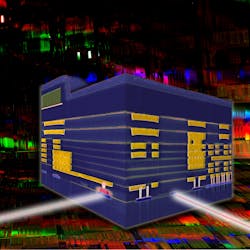
At the IEEE International Electron Devices Meeting in December 2012, IBM described fabrication of the first such module using complementary metal-oxide semiconductor (CMOS) technology with 90 nm geometry.2 The module included four coarse WDM channels spaced 850 GHz apart in the 1500–1550 nm range and filters with flat tops 500 GHz wide. Detection was with a germanium photodiode, compatible with CMOS processing, having 3 dB input bandwidth of more than 20 GHz, and followed by a transimpedance amplifier, limiting amplifiers, and an output buffer.
"All the functions are on the chip except the laser, which is the optical power supply," says Vlasov. Input signals are coupled into the module through the germanium photodiode, and an external continuous-wave laser is an "optical power supply" coupled to the transmitter through the modulator (see Fig. 1). The module also includes WDM filters, waveguides, crossings, directional couplers, and vertical grating couplers.
In addition to benefitting from billions of dollars invested in silicon technology, Vlasov says the IBM approach also benefits from two other factors. Use of a single die allows standard pick-and-place assembly techniques, greatly reducing packaging costs. The design also accommodates standard microelectronic techniques that can test components during assembly, before costly packaging is finished.
Looking forward to 400 Gigabit Ethernet, Vlasov envisions transmitting 25 Gbit/s signals on 16 channels spaced more closely, but still allowing operation at temperatures of 0° to 70°C without significant crosstalk. He says scaling from 100 to 400 Gbit/s "is a question of design rather than technology."Hybrid silicon photonics
An alternative approach is molecular bonding of III-V gain material directly to the silicon, adding light sources and gain to the CMOS silicon platform, plus offering new options for modulation and detection. Adding the III-V material requires steps outside the standard silicon processing, but also integrates the two more tightly. Most work has focused on indium phosphide materials for 1.3 or 1.55 μm bands.
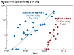
"Hybrid silicon now has the same performance as pure indium phosphide," says Martijn Heck of the University of California at Santa Barbara (UCSB; Santa Barbara, CA). The number of components integrated on InP substrates has been doubling every 2.6 years, but hybrid silicon integration has been doubling every year since the first demonstration less than a decade ago, two decades after the first InP integration (see Fig. 2).3
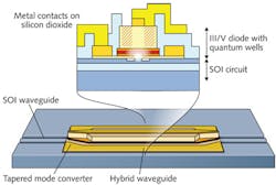
So far, the best developed hybrid silicon photonics are fabricated on silicon on insulator (SOI) substrates (see Fig. 3). Bonding the III-V junction just above a silicon waveguide creates a hybrid waveguide that couples light generated in the III-V active region into a different mode that resides entirely within the silicon. In a postdeadline paper at the Conference on Optical Fiber Communications in March 2013, Aurrion (Goleta, CA) reported hybrid silicon integration, incorporating both an array of eight uncooled 1.3 μm band lasers fixed at 200 GHz intervals for data communications, and a tunable laser in the 1.55 μm band for telecommunications.4 In the same session, Skorpios Technologies (Albuquerque, NM) described its own tunable hybrid silicon laser in the 1.55 μm band. Intel (Santa Clara, CA) has demonstrated what it calls "a fully functional" hybrid silicon photonics module operating at 100 Gbit/s.5John Bowers' group at UCSB also is developing a new generation of hybrid silicon photonics based on silica-on-silicon technology, which allows fabrication of silicon nitride waveguides with as low as 0.05 dB/m and other higher-performance components including array waveguides (AWGs) and ring-filter arrays. At the OFC 2013 postdeadline session, UCSB described a 400 Gbit/s WDM receiver made with that approach. They fabricated a low-loss silicon nitride strip waveguide sandwiched between silica layers to make an array waveguide capable of demultiplexing eight channels separated by 400 GHz, then added InGaAs photodetectors capable of detecting 50 Gbit/s. That allowed the module to process a 400 Gbit/s signal.6
"This opens a new perspective for applications," says Heck. "We are working on microwave photonics, narrowband radio-frequency generators with low phase noise." The ultra-low-loss waveguide technology also benefits development of narrow-line or ultrastable modelocked lasers. In principle, it could allow development of integrated ring resonators with Q factors of a few hundred million. The AWG could be combined with III-V optical amplifiers to make oscillators with multiple output wavelengths. Silicon photonics were conceived for data center communications, but with performance now on a par with indium phosphide, Heck says, "more high-performance telecommunications applications are within reach."
UCSB also is developing free-space beam-steering silicon photonics for DARPA's Sweeper project. Large-scaled phased arrays of grating emitters with their beams emitting from the chip surface would be steered by electro-optical phase modulators a few orders of magnitude faster than conventional MEMS devices. Although power would be limited, the technology could be useful in inter-chip data links.
Defining silicon photonics for the future
Many challenges remain for silicon photonics. The tradeoffs between silicon and III-V components are still being explored. Although CMOS-based silicon fabrication technology is far more mature and economical, III-V materials offer better speed and performance in components including modulators and detectors. How well can the silicon components meet the high performance requirements of telecommunications?
Current silicon photonics is limited by temperature sensitivity of components such as resonators or filters. Developers are exploring how to reduce their temperature sensitivity, and to reduce power consumption of the silicon components that generate much of the troublesome heat. The heat generation that led to multicore chips may limit the use of silicon photonics to link cores or chips.
Nonetheless, silicon photonics are being written into standards aimed at data centers, where they can deliver much-needed high-speed interconnections. The technology is a serious contender for future telecommunications systems and for other low-power applications in sensing and beam direction.
REFERENCES
1. Y. A. Vlasov, "Silicon CMOS-integrated nano-photonics for computer and data communications beyond 100G," IEEE Communications Magazine, 567–572 (Feb. 2012).
2. S. Assefa et al., "A 90nm CMOS integrated nano-photonics technology for 25Gbps WDM optical communications applications," IEEE International Electron Devices Meeting (IEDM), postdeadline session 33.8, (December 10–12, 2012).
3 M. J. R. Heck et al., "Hybrid silicon photonic integrated circuit technology," IEEE J. Sel. Topics Quant. Electron. V, 19, 6100117 (Jul./Aug. 2013); doi:10.1109/JSTQE.2012.2235413.
4. B. R. Koch et al., "Integrated silicon photonic laser sources for telecom and datacom," OFC/NFOEC 2013, postdeadline paper PDP5C.8.
5. E. Marchena et al., "Integrated tunable CMOS laser for Si photonics," OFC/NFOEC 2013, postdeadline paper PDP5C.7.
6. M. L. Davenport et al., "A 400 Gb/s WDM receiver using a low loss silicon nitride AWG integrated with hybrid silicon photodetectors," OFC/NFOEC 2013, postdeadline paper PDP5C.5.
7. M. J. R. Heck, M. L. Davenport, and J. E. Bowers, "Progress in hybrid-silicon photonic integrated circuit technology," SPIE Newsroom, doi:10.1117/2.1201302.004730 (2013).

Jeff Hecht | Contributing Editor
Jeff Hecht is a regular contributing editor to Laser Focus World and has been covering the laser industry for 35 years. A prolific book author, Jeff's published works include “Understanding Fiber Optics,” “Understanding Lasers,” “The Laser Guidebook,” and “Beam Weapons: The Next Arms Race.” He also has written books on the histories of lasers and fiber optics, including “City of Light: The Story of Fiber Optics,” and “Beam: The Race to Make the Laser.” Find out more at jeffhecht.com.


