Red laser diode miniaturization improves printing applications
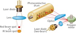
Oclaro (San Jose, CA) engineers have dramatically miniaturized their red laser diodes: Four-beam devices have decreased in volume by 75% (from TO 9.0 mm can packages to TO 5.6 mm cans) and eight-beam devices have shrunk 80% (from TO 16.0 to TO 9.0 mm cans). The size reductions—all while maintaining previous output power levels of around 5 to 15 mW per channel, respectively, depending on the application—will enable designers creating laser beam printers (LBPs) and multifunction printers (MFPs) to design smaller and more compact printers or to use the extra space for adding more features and functionality.
Miniaturization of the 650–680 nm red multi-laser-diode devices was achieved by using small laser diode chips separated individually by an air-ridge structure and by applying a high-reflectivity coating on the diode facet. High-accuracy mounting with low assembly stress and junction-down die bonding results in low droop (the drop in power due to thermal heating of the laser diode once voltage is applied) and narrow beam pitch on the order of 30 to 50 μm. Contact Gunnar Stolze at [email protected].

Gail Overton | Senior Editor (2004-2020)
Gail has more than 30 years of engineering, marketing, product management, and editorial experience in the photonics and optical communications industry. Before joining the staff at Laser Focus World in 2004, she held many product management and product marketing roles in the fiber-optics industry, most notably at Hughes (El Segundo, CA), GTE Labs (Waltham, MA), Corning (Corning, NY), Photon Kinetics (Beaverton, OR), and Newport Corporation (Irvine, CA). During her marketing career, Gail published articles in WDM Solutions and Sensors magazine and traveled internationally to conduct product and sales training. Gail received her BS degree in physics, with an emphasis in optics, from San Diego State University in San Diego, CA in May 1986.
