Germanium-tin laser for silicon photonics is CMOS compatible
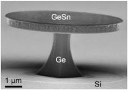
At the IEEE International Electron Devices Meeting (IEDM) 2015 (7 to 9 December, 2015; Washington, DC) a team from several European research organizations and universities, led by the Forschungszentrum Jülich institute (Rostock, Germany), will report on a silicon-based direct-bandgap germanium-tin (GeSn) microdisk laser that emits at a lasing wavelength of 2.5 μm at a power output of 221 kW/cm2.1
The device was built using standard CMOS-compatible processing and was monolithically integrated on a silicon platform. Its 560-nm-thick GeSn epitaxial layers were grown on Ge buffers/Si substrates. Its lasing performance arises from 1) straining the epitaxial layers so they become direct bandgap materials; and 2) its microdisk cavity architecture. The work is an important step toward integrated silicon photonics, as creating CMOS-compatible light sources has proven to be difficult for integrated photonics.
In the fabrication process, after epitaxy, the microdisk mesa is defined using a dry-etch process, then is undercut using a tetrafluoromethane (CF4) plasma. The disks are then passivated with an aluminum oxide (Al2O3) layer. Strain relaxation occurring towards the disk edge is said to lead to better performance.
Source: IEDM 2015
REFERENCE:
1. Stephan Wirths et al., Paper 2.6, "Direct Bandgap GeSn Microdisk Lasers at 2.5 µm for Monolithic Integration on Si-Platform," Forschungszentrum Jülich/ Paul Scherrer Institute/ETH/University of Leeds/University of Grenoble/CEA LETI Minatec.

John Wallace | Senior Technical Editor (1998-2022)
John Wallace was with Laser Focus World for nearly 25 years, retiring in late June 2022. He obtained a bachelor's degree in mechanical engineering and physics at Rutgers University and a master's in optical engineering at the University of Rochester. Before becoming an editor, John worked as an engineer at RCA, Exxon, Eastman Kodak, and GCA Corporation.
