Pulsed laser ablation improves holographic lens fabrication
Researchers from the University of Birmingham in England and Harvard Medical School and Wellman Center for Photomedicine (Boston, MA) have developed a one-step rapid holographic recording technique based on a nanosecond laser pulse that enables optical structures to be printed on transparent substrates coated with light-absorbing materials.
Although laser machining is mostly used for the production of micron-scale objects, it may also be useful for the fabrication of large-area optically active nanopatterned surfaces using laser-interference-assisted ablation (holographic laser ablation).
RELATED ARTICLE: Holographic interferometry: A funny thing happened on the way to the patent office
In laser ablation, material is removed from a solid surface by irradiation with a laser beam. Instead of using a focused laser beam (which produces micron-scale features), the technique implements laser-interference patterns to ablate surfaces and produce interesting nanoscale features.
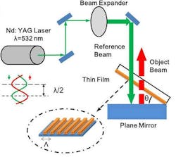
In the single-step rapid holographic-recording technique, a pulsed laser beam irradiates the thin semi-absorbing material used as a glass-substrate coating. This beam passes through the sample and is reflected back from the mirror below. Interference then occurs between the two laser beams traveling in opposite directions, resulting in an interference pattern that ablates a well-ordered grating onto the surface.
The period of the grating is determined by the incident wavelength (λ) and tilt angle (θ) of the sample with respect to normal incidence. The constructive interference is produced at intervals of λ/2, showing the effect of a stationary wave.
This method is both flexible and fast compared with traditional laser-ablation techniques. By simply changing θ, the periodicity of gratings can be tailored and a variety of materials can be patterned. The fabricated gratings have a feature size comparable to the wavelength of visible light and therefore show strong diffraction effects, causing them to appear colorful. This feature makes them suitable for use as security holograms.
The technique is much faster and more economically efficient than conventional nanofabrication methods such as electron-beam lithography and photolithography. The process is also simpler compared with direct laser interference patterning, in which a single pulsed beam is divided using beam splitters and then recombined to produce holograms and nanopatterns. This latter approach requires precise alignment of various laser beams and suffers from low light intensity after beam splitting. This method, on the other hand, uses a single-pulsed laser beam for the rapid printing of nanopattern/holograms on flat or curved surfaces.
The researchers have also demonstrated that this method can be used for printing 2D complex patterns, such as concentric arrays of rings. This capability makes the technique useful for the fabrication of optical devices such as Fresnel zone plates (FZPs), which consist of a concentric array of opaque and transparent rings. Because FZP lenses are flat and lightweight, they are widely used for astronomical applications and in compact optical systems. However, fabrication of FZPs via conventional methods necessitates the use of many process steps, chemicals, and expensive equipment. Alternatively, this holographic-laser-ablation method enables the production of ultra-thin FZPs within seconds.
The team is now working to produce more sophisticated nanopatterns such as grids, triangular arrays, and 3D geometries using the same technique and is also exploring further applications in areas such as data storage and biosensing.
SOURCE: SPIE Newsroom; http://spie.org/newsroom/technical-articles/6194-holographic-lens-fabrication-using-laser-ablation?highlight=x2400&WT.mc_id=KNRNANOE

Gail Overton | Senior Editor (2004-2020)
Gail has more than 30 years of engineering, marketing, product management, and editorial experience in the photonics and optical communications industry. Before joining the staff at Laser Focus World in 2004, she held many product management and product marketing roles in the fiber-optics industry, most notably at Hughes (El Segundo, CA), GTE Labs (Waltham, MA), Corning (Corning, NY), Photon Kinetics (Beaverton, OR), and Newport Corporation (Irvine, CA). During her marketing career, Gail published articles in WDM Solutions and Sensors magazine and traveled internationally to conduct product and sales training. Gail received her BS degree in physics, with an emphasis in optics, from San Diego State University in San Diego, CA in May 1986.
