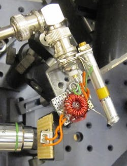
Boulder, CO--A group at JILA has developed a laser-based source of terahertz radiation that is unusually efficient and less prone to damage than similar systems.1 The technology might be useful in applications such as detecting trace gases or imaging weapons in security screening.
Terahertz radiation is useful because many substances have unique absorption characteristics at such wavelengths; however, terahertz systems are challenging to build because they require a blend of electronic and optical methods.
The JILA technology is a new twist on a common terahertz source, a semiconductor surface patterned with metal electrodes and excited by ultrafast laser pulses. An electric field is applied across the semiconductor while a train of 70 fs near-IR pulses with an 89 MHz repetition rate dislodge electrons from the semiconductor. The electrons accelerate in the electric field and emit terahertz radiation.
The innovations eliminate two known problems with these devices. Adding a layer of silicon dioxide insulation between the gallium arsenide semiconductor and the gold electrodes prevents electrons from becoming trapped in semiconductor crystal defects and producing spikes in the electric field. Causing the electric field to oscillate rapidly by applying a radio-frequency signal ensures that electrons generated by the light cannot react quickly enough to cancel the electric field.
Higher power without damage
The result is a uniform electric field over a large area, enabling the use of a large laser-beam spot size and enhancing system efficiency. Significantly, users can boost terahertz power by raising the optical power without damaging the semiconductor. Sample damage was common with previous systems, even at low power. Among other advantages, the new technique does not require a microscopically patterned sample or high-voltage electronics. The system produces a peak terahertz field (20 V/cm for an input power of 160 mW) comparable to that of other methods.
While there are a number of different ways to generate terahertz radiation, systems using ultrafast lasers and semiconductors are commercially important because they offer an unusual combination of broad frequency range, high frequencies, and high intensity output.
NIST has applied for a provisional patent on the new technology. The system currently relies on a large Ti:sapphire laser but could be made more compact by use of a different semiconductor and a smaller fiber laser, says senior author Steven Cundiff, a NIST physicist.
JILA is a joint institute of the National Institute of Standards and Technology (NIST) and the University of Colorado at Boulder.
REFERENCE:
1. H. Zhang et al., Optics Letters, Jan. 15, 2011.
Subscribe now to Laser Focus World magazine; it's free!

John Wallace | Senior Technical Editor (1998-2022)
John Wallace was with Laser Focus World for nearly 25 years, retiring in late June 2022. He obtained a bachelor's degree in mechanical engineering and physics at Rutgers University and a master's in optical engineering at the University of Rochester. Before becoming an editor, John worked as an engineer at RCA, Exxon, Eastman Kodak, and GCA Corporation.