SCAM crystal substrate is better than sapphire for GaN-based LEDs
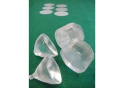
Fukuda Crystal Laboratory (Sendai, Japan) has created 2-in.-diameter samples of a crystal it hopes will replace sapphire for use as gallium nitride (GaN)-based LEDs and laser diodes: scandium aluminum magnesium oxide (ScAlMgO4, or SCAM). As Tech-On! reports, SCAM leads to a reduction in crystal defects for GaN-based semiconductors grown on it. As a result, SCAM is expected to improve the brightness of GaN-based light-emitting devices.
A research group led by Takashi Matsuoka, professor at the Institute for Materials Research at Tohoku University (also in Sendai), formed an LED structure by using the prototype crystal as a base for stacking GaN-based semiconductor layers, the crystal did indeed improve the crystal structure of the GaN.
1.8% lattice mismatch
The lattice mismatch between SCAM and GaN is as small as 1.8%, and SCAM reduces the appearance of crystal defects called dislocations. Though SCAM crystals are difficult to make, Fukuda Crystal Laboratory created 2-in. high-quality SCAM crystals using the Czochralski (CZ) method. It improved crystal quality by modifying the CZ furnace structure and the conditions for crystal growth.
When the prototype SCAM crystal was cleaved and its C surface examined by X-ray diffraction, the full width at half maximum (FWHM) scatter was only 12.9 seconds -- equivalent to that produced by a perfect crystal of silicon (Si).
Fukuda Crystal Laboratory formed the wafers simply by cleaving an ingot of SCAM crystal without resorting to cutting or polishing, reducing the potential cost of wafer fabrication. When a GaN thin film was grown on the cleaved surface of the SCAM crystal using metal-organic chemical vapor deposition at a temperature of 1040°C, a low-dislocation crystal having a mirror surface was formed. The company considers this as a major achievement.
Fukuda Crystal Laboratory plans to increase the diameter of the SCAM crystals as well as commercialize the process. Specifically, it intends to release a 2-in.-diameter SCAM substrate by the spring of 2015.
Source: http://techon.nikkeibp.co.jp/english/NEWS_EN/20140820/371613/

John Wallace | Senior Technical Editor (1998-2022)
John Wallace was with Laser Focus World for nearly 25 years, retiring in late June 2022. He obtained a bachelor's degree in mechanical engineering and physics at Rutgers University and a master's in optical engineering at the University of Rochester. Before becoming an editor, John worked as an engineer at RCA, Exxon, Eastman Kodak, and GCA Corporation.
