PHOTOVOLTAICS: New lasers advance efficiency and manufacture of silicon-wafer-based photovoltaic solar cells
KLAUS STOLBERG, PETER OESTERLIN, and GABRIELE EBERHARDT
The photovoltaic (PV) industry is faced with a number of challenges. One major task is cost-reduction of the solar cells or modules, while another is enhancement of module efficiency. Thin-film technologies seem to win the race for the lowest price-per-watt, but crystalline (wafer-based) solar cells exhibit the highest efficiency. Commercially available monocrystalline-silicon cells currently achieve 12% to 19% efficiency, which is still a long way from the theoretical goal of 35%. Losses are caused by light reflection, carrier recombination, ohmic losses, shadowing effects of the front contacts, and so forth. New cell concepts are aimed at finding solutions to reduce these losses.
Backside contacts
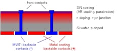
On the front plane of a typical solar cell, for instance, front contact patterning—which can take up to 10% of the complete area—"shadows" the photoactive area, thereby reducing the output of the cell. This effect can be reduced if the contacts are taken through to the backside of the solar cell: "metal wrap through" (MWT) and "emitter wrap through" (EWT) are technological approaches to accomplish this. In both cases 50 to 100 µm via holes must be drilled through 160- to 200-µm-thick silicon wafers. The back contacts can be accessed from the backside, as well as (former) frontside contacts (see Fig. 1). This offers advantages for the electrical connections to the cell and resistance (ohmic) losses are reduced because the dimensions of the contacts at the backside are no longer limited by shadowing effects.
The MWT technology requires that about 100 holes be drilled, typically within one to two seconds. For EWT technology the hole size is smaller, but about 10,000 holes must be drilled at the same rate. Today's laser technology can fit both demands, but only MWT solar cells have already been seen in the market in small numbers (from Photovoltech, Kyocera, Sunway). Efficiency of commercial MWT cells is about 1% higher than that of conventional cells.
One critical point is to reach a high throughput by finding the best combination of all laser parameters together with focusing conditions and synchronization of the laser trigger with beam deflection. It is known that the best ablation rate (and thus fastest drilling) in silicon is reached using a pulse duration of about 100 ns. 1 A hot desire of the application engineer is to have a laser source available in the process development that allows the pulse duration to be adjusted independent of the repetition rate and pulse energy. Jenoptik has introduced such a laser, named JenLas disk IR50.
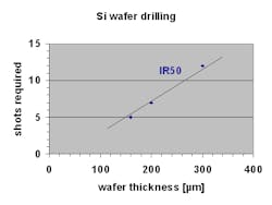
Drilling of MWT holes was systematically investigated with this laser. With the best pulse length of about 1500 ns only five to seven laser shots are required for a complete drill-through of a 180 µm silicon wafer (see Fig. 2). If laser power is further enhanced, the number of necessary laser shots can be reduced to three or four.Selective doping
Even without using the back contact cell concept, there are other opportunities to enhance cell efficiency. Within the frame of classical cell structure with frontside and backside contacts, laser diffusion or laser doping is a "hot" topic in crystalline solar-cell manufacturing.
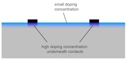
So-called "selective doping" of the silicon allows reduction of the electrical resistance (ohmic losses) of the bulk silicon material underneath the contact fingers. An increase of absolute cell efficiency of 0.3% to 0.5% has been demonstrated using this method. In this process a phosphorus coating diffuses from the surface into the bulk silicon at the locations where the silicon is melted by the laser. This location is identical to the where the contact fingers are later located. The sheet resistance of the laser-treated area is strongly reduced, compared to the nontreated area, from 120 to 150 ohm/sq to 20 ohm/sq, for instance (see Fig. 4).Different laser types and wavelengths have been tested, from IR to the UV. Infrared lasers are available with very high power, but the penetration depth of the radiation in silicon is largeµseveral hundred micronsµso a lot of laser power is lost in heating the bulk material of the wafer. Additionally there are indications that IR lasers generate more lattice defects than shorter-wavelength lasers.
At the other end of the spectral range, UV lasers are well suited for laser diffusion due to the high absorption in a very shallow surface layer. However the available laser power in the UV is limited to typically 20 W, which is insufficient for production rate throughput.
Green offers a good compromise. The optical penetration depth of roughly 1 µm is well suited for a thermal process 0.5 µm deep, and the available laser power ranges are above 100 W, which is sufficient for production-rate throughput. With CW frequency-doubled solid-state lasers it is easy to focus the beam to a spot size as small as 20 to 40 µm and scan it at high-speed over the wafer surface, using galvo scanners. However, the process time, given by the ratio of the spot diameter and the scan speed, is typically in the range of 20 to 100 µs. Within this period a lot of heat diffuses into the bulk material of the wafer, as the heat diffusion length for such a process time is 30 to 60 µm. An estimate shows that for a production rate of 1 wafer per second a total CW laser power of at least 600 to 800 W would be needed, much beyond what is suitable for a production tool concept.
In contrast Q-switched solid-state lasers deliver pulses of 300 ns or less duration. The heat diffusion length is only 3.5 µm, about 10% of that for the CW laser process. With these lasers the same production rate can be achieved with roughly 200 W of laser power, which is feasible for 24/7 production equipment. Laboratory results with the JenLas ASAMA or with other lasers are very promising, indicating that this process proposal is not far from implementation in production halls.4, 5
The question about the additional manufacturing costs can also be answered positively. With an increase of 0.3% absolute efficiency for crystalline cells the additional laser process "pays for itself," meaning that the depreciation and operating costs of the laser production tool would be compensated by the higher efficiency (and thus higher payback) of the cells.
The process is basically known, but tool concepts must be developed to bring the process onto the production line. Handling of thin and fragile wafers (typical thickness 180 µm) is required as well as simple and reliable beamsplitters and beam-shaping concepts that divide a single laser beam into as many spots as contact fingers are needed. The feeding of wafers into the machine must be optimized so that the loading/unloading time of the wafers is minimized. Additionally the wafers must be aligned properly to the laser diffusion process because the laser treated lines must match with the contact fingers which are applied in a subsequent process step.
All these processing concepts enhance solar cell efficiency and can be integrated into the JENOPTIK-VOTAN Solas 1800 machine—a new professional laser tool that allows wafer processing up to 1800 wafers/h. Wafer position control is an item as well as feed-stocking, safe ablation exhaust, quality control by image processing and full automation to fulfill 24/7 demand. The system is offered in two versions, stand-alone for development of new products and processes, and a technology module for integration into an existing in-line production system.
REFERENCES
1. M. Leitner, E. Körner, Stuttgarter Lasertage, Proc. Stuttgart (2003).
2. F. Book et al., Proc. 23rd EC PVSEC, Sept. 1-5, 2008, Valencia.
3. K. Neckermann et al., 22nd EPSEC, Sept. 3-7, 2007, Milano.
4. M. Okanovic et al., Proc. 24th EUPVSEC, 2009, Hamburg, Germany.
5. J.R. Köhler et al., Proc. 24th EUPVSEC, 2009, Hamburg, Germany.
KLAUS STOLBERG is manager of industrial laser applications with JENOPTIK Laser, Optik, Systeme, PETER OESTERLIN is general manager at Innovavent, and GABRIELE EBERHARDT is head of application photovoltaic/electronics with JENOPTIK Automatisierungstechnik; e-mail: [email protected]; www.jenoptik.com.


