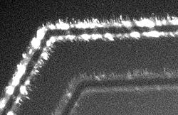
Gaithersburg, MD--While refining a novel method they developed for making nanowires, chemists at the National Institute of Standards and Technology (NIST) discovered a new way to create nanowires that produce light similar to that from LEDs.1 The emitters could eventually be used as nanoscale light sources, for example in lab-on-a-chip systems.
Nanowires are typically grown by chemical vapor deposition (CVD). Most CVD techniques form nanowires that rise vertically from a surface. Because the wires only contact the substrate at one end, they tend not to share characteristics with the substrate material--a less-than-preferred trait because the exact composition of the nanowires will then be hard to define. Vertical growth also produces a dense forest of nanowires, making it difficult to find and reposition individual wires of superior quality.
Surface-directed growth
Two years ago, NIST chemists Babak Nikoobakht and Andrew Herzing remedied these shortcomings, unveiling a "surface-directed" method for growing nanowires horizontally across a substrate. Like many vertical-growth CVD methods, the NIST fabrication technique uses gold as a catalyst for crystal formation. The difference is that the gold deposited in the NIST method is heated to 900 degrees C, converting it to nanoparticles that serve as growth sites for the crystallization of zinc oxide molecules. As the zinc oxide nanocrystals grow, they push the gold nanoparticles along the surface of the substrate (in this experiment, gallium nitride) to form nanowires that grow horizontally across the substrate, thus exhibiting properties strongly influenced by the base material.
Modification creates light
Now, Nikoobakht and Herzing have increased the thickness of the gold catalyst nanoparticles from less than 8 nm to approximately 20 nm. The change results in nanowires that grow a secondary structure--a "nanowall" in which the zinc oxide portion is electron-rich and the gallium nitride portion is electron-poor. The resulting p-n heterojunction produces light when a voltage is applied across the nanowire-nanowall combination. This led the researchers to dub the structure a "nano LED."
Unlike previous techniques for producing heterojunctions, the NIST surface-directed fabrication method makes it easy to locate individual heterojunctions on the surface. This feature is especially useful when a large number of heterojunctions must be grouped in an array to form a light-emitting unit.
Transmission-electron-microscope (TEM) examination of the zinc oxide / gallium nitride nanowires and nanowalls revealed few structural defects in the nanowires and very distinct p-n heterojunctions in the nanowalls, both affirmations of the effectiveness of the NIST surface-directed fabrication method.
Nikoobakht and Herzing want to improve the nano LEDs by using better geometry and material designs.
REFERENCE:
1. B. Nikkoobakht and A. Herzing, ACS Nano, published online Sept. 15, 2010.
Subscribe now to Laser Focus World magazine; it’s free!

John Wallace | Senior Technical Editor (1998-2022)
John Wallace was with Laser Focus World for nearly 25 years, retiring in late June 2022. He obtained a bachelor's degree in mechanical engineering and physics at Rutgers University and a master's in optical engineering at the University of Rochester. Before becoming an editor, John worked as an engineer at RCA, Exxon, Eastman Kodak, and GCA Corporation.
