LIGHT-EMITTING DIODES: LED source emits entangled photon pairs
The future of quantum information is about to improve due to the development of a breakthrough LED from researchers at Toshiba Research Europe Limited (Cambridge, England) that generates entangled photon pairs.1 To date, optical quantum-computing applications have been limited by the bulky and complex components of the lasers and optics required to generate entangled photons.
Electrically injected
This is the first demonstration of a solid-state, electrically driven device consisting of a quantum dot embedded in a semiconductor LED structure that emits entangled photon pairs (from either AC or DC electrical injection) with a purity more than sufficient to meet the needs of future, scalable quantum-information applications. Other single-photon LEDs based on quantum dots are also being developed and could potentially generate entangled photons indirectly; however, the entangled LED does so directly and is far easier to implement.
A single quantum dot
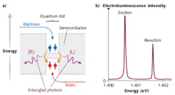
The key ingredient of the Toshiba entangled LED (ELED) is a single quantum dot that, as previous research has shown, can be manipulated to emit single pairs of entangled photons through radiative decay of its biexciton state (see figure). A biexciton is two weakly bound excitons, an exciton being the bound state of an electron and an electron hole. Essentially, electrical injection into the quantum dot creates the biexciton state through the capture of two electrons and two holes. This biexciton state radiatively decays to the ground state, producing a pair of photons with a polarization state that depends on the decay parameters. For example, though the polarization of the first photon is unknown until measured, the second will be oppositely circularly polarized. Only certain quantum dots (when the wavelength of the photons is independent of polarization) emit entangled light. The dots can be produced by controlling their size carefully during wafer growth.
To generate large numbers of entangled pairs, the overall ELED device consists of a single layer of quantum dots embedded in the p-i-n structure of the semiconductor layers. The 400 nm thick intrinsic region of the structure prevents electrons from tunneling into the quantum-dot core from the n-doped region during biexciton decay, minimizing destruction of entangled states.
Analysis of the entangled photon pairs upon DC electrical injection with a current density of 31 nA/μm2 shows entanglement fidelity–the purity of entangled light–of 70.7% ± 2.3%. Because this value exceeds the fidelity limit of 50% by nine standard deviations for a source emitting a classically polarization-correlated state, it proves that this ELED produces entangled photons (uncorrelated light has a fidelity value of 25%).
By pulsing the ELED with an AC input at 80 MHz, the emission of entangled light can be controlled for an improved fidelity value of 78.5%. The fidelity is increased even further to 82.6% by controlling the maximum permitted time delay between two photons to register a detection event, known as the gate width of the device, to 0.1 ns.
"We were pleased to discover that the performance of the ELED is comparable to its optically excited cousins, so there is no tradeoff between the convenience of electrical injection and quality of entangled light," says Mark Stevenson, senior research scientist at Toshiba Research Europe Ltd. "We hope with further refinement, integration of many ELEDs on a single chip will be key to realizing practical quantum circuits and a useful quantum computer."
REFERENCE
1. C.L. Salter et al., Nature, 465, 594-597 (June 3, 2010).

Gail Overton | Senior Editor (2004-2020)
Gail has more than 30 years of engineering, marketing, product management, and editorial experience in the photonics and optical communications industry. Before joining the staff at Laser Focus World in 2004, she held many product management and product marketing roles in the fiber-optics industry, most notably at Hughes (El Segundo, CA), GTE Labs (Waltham, MA), Corning (Corning, NY), Photon Kinetics (Beaverton, OR), and Newport Corporation (Irvine, CA). During her marketing career, Gail published articles in WDM Solutions and Sensors magazine and traveled internationally to conduct product and sales training. Gail received her BS degree in physics, with an emphasis in optics, from San Diego State University in San Diego, CA in May 1986.
