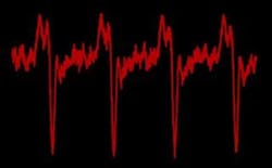
Laser from NIST/JILA directly produces picosecond dark pulses
Boulder, CO--Researchers at the National Institute of Standards and Technology (NIST) and JILA, a joint institute of NIST and the University of Colorado at Boulder, have demonstrated a pulsed quantum-dot (QD) laser that generates sustained streams of "dark pulses," which in terms of intensity versus time are the inverse of ordinary laser pulses.1
The dark-pulse laser is envisioned as a tool for IR communications and measurements. The laser's ultrashort pulses are just 90 ps long. Dark pulses could be useful in signal processing because, unlike bright pulses, they generally propagate without distortion, according to NIST/JILA. Dark pulses might be used like a camera shutter for a continuous-wave (CW) light beam in optical networks.
No subsequent pulse-shaping needed
The new NIST/JILA technology is the first to generate dark pulses directly from a semiconductor laser cavity without subsequent electrical or optical shaping. The QDs are all about 10 nm in size and thus all emit light at the same frequency. The new laser depends on the QDs' unusual energy dynamics, which have the effect of stabilizing dark pulses. After emitting light, QDs recover energy from within rapidly (in about 1 ps) but more slowly (in about 200 ps) from energy inputs originating outside the QDs in the laser cavity. This creates a progression of overall energy gains gradually giving way to overall energy losses. Eventually, the laser reaches a steady state of repeated brief intensity dips--a drop of about 70%--from the CW pump light.
The dark-pulse laser was developed through close collaborations between NIST experts in QD growth and semiconductor laser design and fabrication, and JILA experts in ultrafast lasers and related measurements. NIST has ongoing research efforts to develop QD lasers and to develop modeling, fabrication, and measurement methods for QDs and other semiconductor nanostructures. In general, semiconductor lasers are being considered for many advanced applications, such as next-generation atomic clocks based on optical frequencies, for which large lasers are costly and complex.
REFERENCE:
1. M. Feng et al., Optics Express, published online June 7, 2010, as forthcoming.

John Wallace | Senior Technical Editor (1998-2022)
John Wallace was with Laser Focus World for nearly 25 years, retiring in late June 2022. He obtained a bachelor's degree in mechanical engineering and physics at Rutgers University and a master's in optical engineering at the University of Rochester. Before becoming an editor, John worked as an engineer at RCA, Exxon, Eastman Kodak, and GCA Corporation.
