MATERIALS PROCESSING: Excimer lasers boost performance of diamond-like carbon films
Diamond has both the highest hardness and thermal conductivity of any known material. As a result, the ability to deposit thin diamond films, or more specifically, diamond-like carbon (DLC) films, has potential use in many applications in which product durability, wear resistance, or heat control are critical. The technology currently used to produce DLCs for products such as razor blades yields relatively thin films with poor adhesion that are not adequate for more demanding uses, such as might be found in the automotive industry. Now, a new excimer-laser-based technique has been developed that offers the ability to achieve thicker films characterized by good adhesion, low internal stress, and high purity—which all translate into increased durability. Furthermore, the excimer technique does not involve heating the substrate, meaning that it can be used with a wide range of materials, including polymers.
What are DLCs?
Carbon can form varying types of crystal lattices. In graphite, for example, each carbon atom is bonded to its three neighbors with covalent bonds. These bonds all lie in a plane and are separated with an angular spacing of 120°, a configuration that’s referred to as sp2 hybridized bonding. Weak electronic forces hold each plane of the lattice together. In diamond, each carbon atom is connected by four covalent bonds to its neighbors, and the lattice has a three-dimensional, tetrahedral form. This is termed sp3 hybridized bonding.
The DLCs exist in a number of different forms; the hardest is called tetrahedral amorphous carbon (ta-C), which ideally consists purely of sp3 bonded carbon atoms. Real-world DLCs, however, always contain at least some fraction of sp2 bonds, and often some atomic impurities like hydrogen. However, a ta-C film having an sp3 content of more than 50% has a hardness of more than 40 GPa and a low friction coefficient, making it highly useful for controlling wear.
A common major mechanical limitation of high-purity ta-C films has been the buildup of internal compressive stress in the coating.1 With existing fabrication methods, this stress has typically limited film thickness to 0.2 µm or less before the risk of delamination from the substrate becomes significant. However, many demanding applications ideally require coatings as thick as 2 µm.
The most obvious way to relieve this stress is through thermal annealing.2 Unfortunately, traditional annealing—bulk heating of the substrate—presents two problems. First, when raised to temperatures above 200°C, sp3 (diamond) films begin to convert into the sp2 (graphite) form. Second, the need for a heating cycle limits the range of substrate materials to those that can withstand high temperatures, ruling out the use of most polymers. Furthermore, from a practical standpoint, the time required for one or more heating and cooling cycles may limit production throughput and increase process cost.
Because of such limitations, commercial use of DLCs has been limited to a few, specialized areas. The single biggest application is currently in increasing the wear resistance of razor blades. These films, which appear black to the eye, are also being used primarily for cosmetic purposes on high-end watches. This black appearance is because graphite has extremely high absorption at visible wavelengths, so even the highest-purity DLCs appear black due to the presence of some graphite.
The ability to produce thicker DLCs on a wider variety of substrate materials would increase their use substantially. In particular, DLCs could enhance the lifetime of many machine tools, and would also be applicable for any high-cost parts that are subject to wear, such as in high-performance automobiles.
The excimer laser process
A new technique uses excimer lasers for both film deposition and rapid-thermal annealing of sub-layers. This two-step process is capable of delivering thick (up to 10 µm) films having no internal stress and high hardness, and can be applied to a wide range of substrates, including temperature-sensitive materials such as polymers.
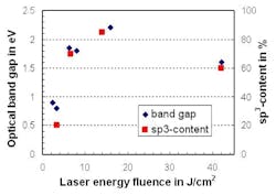
Film growth is accomplished through pulsed laser deposition (PLD). Specifically a high-pulse-energy excimer laser, operating at 248 nm, is used to ablate a graphite target inside a vacuum chamber. This creates a ta-C film on a substrate, which is moderately heated (to <90°C) inside the vacuum chamber. The fast evaporation of the target material induced by the high photon energy (5 eV), short temporal width (30 ns), and high fluence of the excimer laser pulses (many J/cm2) generates atomic species with a high degree of ionization and high kinetic energies. In particular, the mean kinetic energies in the excimer-laser-created plume are in the range of 30 to 80 eV for laser fluences of 5 to 20 J/cm2—significantly higher than the energies associated with thermal evaporation and ion sputtering deposition methods. This is critical, since increasing the kinetic energy of the atoms generally translates into a film with greater tetrahedral (sp3) diamond-like carbon content (see Fig. 1).
However, even when PLD film growth parameters are set to maximize sp3 content and hardness, the ta-C thin films initially exhibit internal compressive stress in the range of 10 GPa. This level of stress will lead to delamination of the film from the substrate and prevent preparation of thicker films for more demanding applications, such as wear-resistant coatings. It has been shown previously that residual stress in ta-C films can be eliminated by UV excimer laser annealing.3 Specifically, irradiation of the ta-C film surface with 100 to 200 excimer laser pulses at 248 nm, and a fluence of 150 to 200 mJ/cm2, leads to stress relaxation without reducing the fraction of sp3 bonds. UV excimer laser annealing has the advantage that only a localized surface layer of some 100 nm in depth is heated rapidly, and stress relaxation occurs in just a few microseconds. Therefore, during irradiation of a surface, the mean substrate temperature undergoes no significant increase. Successive excimer laser deposition and annealing cycles can thus enable the buildup of stress-free, high-hardness ta-C coatings with layer thicknesses in the range of several microns.
Measurement results
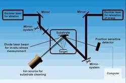
An automated system for performing excimer laser PLD and annealing was constructed utilizing two Coherent LPXpro excimer lasers (see Fig. 2). This particular laser was chosen because it can produce pulse energies up to 1 J, which enables fluences at the target to exceed the optimum values cited previously (10 to 20 J/cm2). It was found that optimum film properties were achieved if the ablation excimer laser was operated with a low-divergence resonator and the annealing excimer laser operated with a standard resonator configuration. With this configuration, 4 µm thick, stress-free, ta-C films can be deposited over an area of 30 cm2 within 60 min. by applying alternating excimer laser ablation and stress relaxation process steps.
Testing data from 2 µm thick, stress-free, high-hardness ta-C films prepared with this optimized setup are summarized in the table. The films were found to be completely amorphous with a density approaching that of diamond, which is the consequence of the high sp3 content. The average surface roughness of films deposited on N1 polished steel substrates was measured with a DEKTAK surface profilometer, and was generally found to be not significantly higher than roughness of the substrate, indicating a very smooth film. Most importantly, extraordinarily high values of hardness and Young’s modulus were measured for 2 µm thick films prepared on both steel and WC hard-metal substrates. The measurements were performed using a dynamic indentation method with a Berkovich indenter according to ISO 14577. The values given in the table are the mean of 10 measurements, each using maximum loads of 50 mN, resulting in maximum indentation depths of about 100 nm.
| Structure | Amorphous |
| sp3 content (%) | 80–85 |
| Optical energy bandgap (eV) | 2.0–2.2 |
| Density (g/cm3) | 3.1–3.3 |
| Internal stress (GPa) | → 0 |
| Avg. surface roughness on N1-polished steel substrates (nm) | 20–30 |
| Hardness (GPa) | 60–65 |
| Young's modulus (GPa) | 880–920 |
| Friction coefficient | 0.10–0.20 |
| Refractive index (visible range) | 2.45–2.55 |
| Extinction coefficient (at 678.3 nm) | 0.015 |
| Extinction coefficient (at 248 nm) | 0.35 |
| Absorption coefficient (at 248 nm) | 1.8 × 105 cm-1 |
Adherence for 2 µm thick ta-C films was also quantified by conventional scratch testing. Since the adherence of the excimer-laser-produced ta-C films on steel substrates was insufficient for some applications, intermediate layers were used. Best adherence was obtained with boron carbide and tungsten carbide intermediate layers, which are also deposited by excimer laser ablation immediately prior to the ta-C deposition. The optimal thickness of these layers depends mainly on substrate roughness, being about 80 nm for N1 polished substrates. This approach yielded maximum critical loads around 35 N for various steels (including 100Cr6, HSS, and nitride steels) with both carbides as intermediate layers, and 55 N for WC hard metal with WC as the intermediate layer. The values of the critical loads at which film damage occurred during scratching are comparable with the adhesion values reported in the literature for currently used DLC coatings. Depending on the PLD parameter settings formation of particulates or droplets can be observed. These particulates consist of graphite, and their size depends on the laser fluence at the target surface. At fluences that were optimal for ta-C film growth, particulate size was on the order of 100 to 200 nm. The number of particulates in the films was minimized by using an unstable resonator along with an optimized laser spot on the target. Research has shown that particulate density in 2.5 µm thick films is generally in the range of 3 × 10⁵ to 2 × 10⁶ per cm2, resulting in an average surface roughness of about 5 to 20 nm, when the ta-C films are deposited on polished silicon of 2 nm average surface roughness.
Commercialization
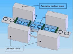
While the excimer-laser-based deposition and annealing method clearly produces high-hardness films with excellent physical characteristics, successful commercial deployment requires that the process meet certain goals in terms of speed and cost. One concept for a high-throughput industrial system utilizes four excimer lasers in a pass-through, in-line arrangement (see Fig. 3). Depending on throughput requirements, high-power excimer lasers with up to 540 W average output power are commercially available.4
This setup is meant for ta-C coating of plane substrates, which are positioned in a rotating carrier. Both the loading and unloading modules act as airlocks, enabling parts to be supplied to the main chamber without ever breaking its vacuum. Furthermore, precleaning of the substrates by ion beam bombardment can be performed in the loading module. The deposition and annealing processes are carried out in the coating module and can be performed simultaneously to maximize throughput. The carriers are rotated in order to bring each part to the proper position, and any number of successive deposition and annealing steps can then be accommodated. When ta-C film deposition is complete, the parts are translated into the unloading module, which can also be used for additional post-processing steps, such as micro-structuring or marking.
Based on the deposition rates achieved in the laboratory, a system like this could produce 0.5 m2 of 1 µm thick ta-C film in 60 min. The total cost per square meter for a continuous process is estimated to be $750, when considering investment costs, consumables, maintenance, electrical energy, and staff.
This excimer-laser-based deposition and annealing method appears to address many of the fabrication problems that have limited adoption of DLCs while also delivering the cost and throughput characteristics required for widespread commercialization.
REFERENCES
1. J. Schwan, S. Ulrich, T. Theel, H. Roth, H. Ehrhardt, P. Becker, S.R.P. Silva, Appl. Phys. Lett. 82, 6024 (1997).
2. T.A. Friedmann, K.F. McCarty, J.C. Barbour, M.P. Siegal, D.C. Dibble, Appl. Phys. Lett. 68, 1643 (1996) .
3. S. Weissmantel, G. Reisse, D. Rost, Surf. Coat. Technol. 188, 268 (2004).
4. R.F. Delmdahl, Superconductor Week 22, No. 23, 5 (2008).
About the Author
Steffen Weißmantel
Steffen Weißmantel is a professor at the University of Applied Sciences Mittweida (Mittweida, Germany).
Günter Reiße
Günter Reiße is a professor at the University of Applied Sciences Mittweida (Mittweida, Germany).
Ralph Delmdahl
Ralph Delmdahl is product marketing manager at Coherent.


