LASER-DIODE FABRICATION: Alignment and etching techniques assist fabrication of edge-emitting laser diodes
CRISTIAN B. STAGARESCU, VINU VAINATEYA, ALFRED T. SCHREMER, ALEX A. BEHFAR, RICH TRAVERS, RODNEY CHISHOLM, AND FRED HAFNER
The reflective mirrors, or facets, at the cavity ends of edge-emitting diode lasers are usually fabricated by mechanical cleaving of semiconductor epi wafers. For most semiconductor materials, however, mechanical cleaving is relatively imprecise and also creates fragile bars and minuscule chips that are awkward to handle during device testing and subsequent operations. Engineers at BinOptics and ASML and have collaboratively addressed these issues by adapting semiconductor manufacturing processes of stepper photolithography to wafer alignment to more efficiently fabricate edge emitting laser (EEL) chips.
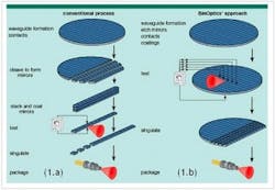
An etched-facet technology (EFT) developed at BinOptics avoids the drawbacks of mechanical cleaving, such as poor yields, while also enabling on-wafer testing, by using photolithography and chemically assisted ion-beam etching (CAIBE) to form the laser facets (see Fig. 1).1 In the EFT process lasers are fabricated on the wafer in much the same way that integrated circuits are fabricated on silicon, which allows the lasers to be monolithically integrated with other photonic devices on a single chip and to be tested inexpensively at wafer level.2, 3 The process has been used to fabricate commercially available indium phosphide (InP)-based lasers with precisely located mirrors, at quality and reflectivity levels equivalent to those obtained by cleaving.4
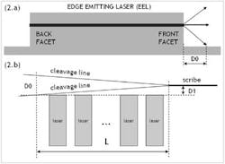
After completion of wafer-level testing, the edge-emitting-laser (EEL) devices need to be separated into chips ("singulated") and individually packaged. The center of the waveguide is located about 3.0 µm above the floor of the CAIBE etch, and typical vertical beam divergence is about 40° FWHM (see Fig. 2). To maintain beam integrity and reduce "clipping" it is desirable when cleaving the laser chip at the front facet to leave only a small patio or lip of excess material. In practice, we have found that a patio no bigger than 5 µm preserves adequate beam quality.In a typical singulation process, a scribe is performed at a lithographically defined distance from the front facets of an array of lasers followed by a "break" step, during which mechanical pressure causes a cleavage line to propagate through the material. Since cleavage lines can propagate laterally from the scribe line, the lithographically defined distance, D1, is set to half of D0 to prevent either clipping of the laser front facet or leaving an excessively large patio or lip on the end of the singulated EEL. As the alignment of the cleavage line improves, the size (L) of the wafer piece that can be singulated in a single step increases also. In practice we require an alignment accuracy of 0.01° (roughly 175 µrad), which for D1 of approximately 2.5 µm results in L of about 14 mm.
Alignment schemes
Singulation can be difficult to achieve, however, because III-V industry wafer flats are typically ground and have a specified alignment to a crystal plane ranging from ± 0.1° for a "standard" flat to ±0.02° for a "precision ground" flat. Neither of these satisfies the ±0.01° alignment requirement, so a better flat is required. For this work, we have used manually cleaved flats on 3 in. indium phosphide (InP) wafers, which provide an ideal reference line along an actual crystal plane. Particularly because the cleaved flat has to be located within just a few mm from the edge of the wafer, however, manual cleaving and breaking does not always yield a perfect line. So to provide the necessary degree of angular alignment, the EFT process begins with the printing of alignment marks in measurable registration to the edge of a known wafer cleavage plane.
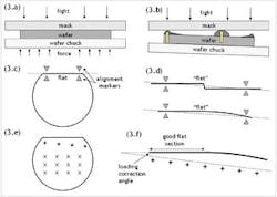
The conventional method for aligning a print matrix to a wafer flat uses a contact mask aligner, in which the wafer is placed on a vacuum chuck, brought into direct physical contact with the mask, aligned, and then printed by direct exposure through the mask-opened areas (see Fig. 3). This method has several drawbacks. One is that any residue on the wafer surface will modify the wafer-to-mask distance and result in uneven print quality. In addition, since the wafer is directly "pressed" into the mask, any residual particle on its surface becomes a high-pressure point, which can result in possible damage or even fracture of the fragile InP wafers.The alignment process involves translating and rotating the wafer until its cleaved edge passes through a pair of "ruler markers" on the contact mask. Manual cleaving and breaking does not always yield a perfect line, and therefore the cleavage line will sometimes jump or bend. Although in practice a good, straight cleaved line segment usually exists on the cleaved edge, the contact mask alignment scheme would sometimes miss it because it can examine the wafer only locally around the marker points.
To avoid these drawbacks we have introduced a two-step "measure-then-correct" alignment procedure that uses the ASML PAS 5500/60 stepper and an external XY-stage vision system. The PAS 5500/60 wafer printing sequence consists of a pre-aligner phase in which the wafer edge is optically "read," followed by loading the wafer onto the exposure stage for the actual exposure. Translation and rotation corrections can be applied to modify the pre-aligner load position.
In our procedure, the wafer is first run through the stepper and a number of alignment marks are printed to form a "calibration" test line near the wafer edge that "imprints" on the wafer the angular loading offset of the pre-aligner stage.5 The cleaved wafer edge and the calibration line of marks are then imaged and mapped in the precision XY-vision system. This results in a detailed map of the entire cleaved edge where we can clearly identify a clean, straight cleaved flat section and measure the "loading offset" angle between this "good flat" and the calibration line. The wafer is then reloaded and the final array of alignment markers is printed with an angular correction equal but opposite to the measured loading offset, thus resulting in a print array well aligned to the "good flat."6
Loading repeatability and alignment results
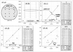
The success of this two-step "measure-then-correct" scheme clearly requires that the PAS 5500/60 pre-aligner stage have a repeatable loading offset. To collect loading offsets statistics and measure repeatability, a 3 in. Si wafer with a standard ground flat and two 3 in. cleaved flat InP wafers have been repeatedly loaded, printed with a row of marks, reloaded, reprinted, and later measured with respect to the flat (see Fig. 4).REFERENCES
1. A. Behfar-Rad et al., Appl. Phys. Lett. 54, 439 (1989).
2. A. Behfar et al., 2005 Optical Fiber Conference, Paper OTuM5.
3. P. Vettiger et al., IEEE J. Quantum Electron. 27, 1319 (1991)
4. A. Behfar-Rad, et al., J. Electrochem. Soc. 136, 779 (1989).
5. M.A. van den Brink, H.F.D. Linders, S. Wittekoek, SPIE 633(08) 1 (March 1986).
6 S. Wittekoek, J. van der Werf, R.A. George, SPIE 538(35) 1 (March 11, 1985).
CRISTIAN B. STAGARESCU is senior engineer, VINU VAINATEYA is staff engineer, ALFRED T. SCHREMER is principal engineer, and ALEX A. BEHFAR is chairman and CEO at BinOptics, 9 Brown Rd, Ithaca, NY 14850; e-mail: [email protected]; www.binoptics.com. RICH TRAVERS is field applications development manager, RODNEY CHISHOLM is major account manager, and FRED HAFNER is field applications development engineer at ASML Netherlands, De Run 6501, 5504 DR, Veldhoven, The Netherlands.


