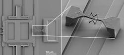
Nanoscribe prints 3D MEMS and microscopic components on integrated circuits
Currently, the production of photonic circuits and microelectromechanical systems (MEMS) needed for communications, transportation, and the medical industry requires different manufacturing methods and multiple process steps for bringing together various components on one microchip. Now, using 3D printers from Nanoscribe (Eggenstein-Leopoldshafen, Germany), companies can print and integrate microscopic components directly on integrated circuits (ICs) such as microlenses onto photonic circuits and deformable structures on MEMS actuators.
RELATED ARTICLE: Low-cost two-photon-polymerization method could enable 3D printing of microstructures within the body
The smallest objects with complex geometry and feature sizes from hundreds of nanometers up to several millimeters can be printed. They are produced in a single printing step using direct laser writing and on a scale that was inaccessible to 3D printing before. This major update of on-chip printing brings new perspectives for producing nano- and microscale 3D components in situ, exactly where needed.
For this 3D printing process, Nanoscribe's Photonic Professional GT system uses the method of two-photon polymerization. Precision optics and advanced software tools allow fabrication of 3D polymer structures with submicron precision, making the strengths of additive manufacturing available to micro and nanofabrication. These advantages are the full 3D design freedom and a simple workflow from CAD model to final part resulting in rapid design iteration cycles that save time and costs during product development. Additionally, the wide choice of print surfaces now also includes pre-patterned chips making miniaturization of 3D functional parts into ICs possible.
Micro-optics are created in one printing step and without the need to align and mount the finished micro-optics mechanically into the pre-structured microchip. This process of direct fabrication of components onto existing circuits reduces packaging costs in equipment and saves time in calibration. Moreover, it avoids pick and place as well as curing-based fixing procedures. Taking advantage of the laser accuracy, 3D microprinting also offers submicron precision and optical quality surfaces meeting the requirements for high performance micro-optics.
Applications in medical imaging, tissue regeneration, and MEMS actuators can benefit from the fabrication of ICs. For example, Nanoscribe customers at Boston University, headed by professor Alice White, fabricated 3D deformable bowtie-like structures directly on MEMS actuators. The 3D printed micromechanical bowties are structures that stretch and deform in 3D due to their geometry. The scientists were able to deform the microstructure by applying a voltage to the MEMS actuator. White says, "We show that coupling 3D microprinting with MEMS actuators is a powerful way to produce 3D micromechanical systems tailored to specific needs. Nanoscribe 3D printers allow us rapid prototyping of submicron-resolution structures that would otherwise be impossible to fabricate via single-photon stereo-lithography or the deposition and etching processes commonly used in semiconductor foundries."
The two-photon polymerization process is the basis for Nanoscribe's 3D microprinting technology. In this printing process a laser exposes a photosensitive resin by means of a high-numerical aperture objective in a controlled trajectory and layer-by-layer following a CAD design. The material solidifies only in the laser focus spot allowing for nearly arbitrary 3D structures with even submicron features.
SOURCE: Nanoscribe; https://www.nanoscribe.de/en/media-press/press-releases/chip-3d-microprinting-photonic-and-mems-systems/

Gail Overton | Senior Editor (2004-2020)
Gail has more than 30 years of engineering, marketing, product management, and editorial experience in the photonics and optical communications industry. Before joining the staff at Laser Focus World in 2004, she held many product management and product marketing roles in the fiber-optics industry, most notably at Hughes (El Segundo, CA), GTE Labs (Waltham, MA), Corning (Corning, NY), Photon Kinetics (Beaverton, OR), and Newport Corporation (Irvine, CA). During her marketing career, Gail published articles in WDM Solutions and Sensors magazine and traveled internationally to conduct product and sales training. Gail received her BS degree in physics, with an emphasis in optics, from San Diego State University in San Diego, CA in May 1986.
