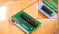
NTU Singapore researchers develop silicon-photonic quantum-communication chip 1000 times smaller than current setups
Most leading security standards (algorithm examples of which include Advanced Encryption Standard, or AES, and Rivest-Shamir-Adleman, or RSA, which are used in making online communications such as payments on shopping websites secure) used in secure communication methods do not take advantage of quantum technology. As a result, electronic transmission of personal identification numbers (PINs) or passwords can be intercepted, posing a security risk.
To mitigate these risks, researchers at Nanyang Technological University, Singapore (NTU Singapore) have developed a silicon-photonics-based quantum-communication chip that is 1000 times smaller than current quantum setups, but offers the same superior security that quantum technology is known for.1 The team is led by NTU professor Liu Ai Qun and associate professor Kwek Leong Chuan.
Roughly 3 mm in size, the chip, which is compatible with the existing fiber-optic communication infrastructure, uses quantum communication algorithms to provide enhanced security compared to existing standards. It does this by integrating passwords within the information that is being delivered, forming a secure “quantum key.” After the information is received, it is destroyed along with the key, making it an extremely secure form of communication.
It also needs 1000 times less space than current quantum communication setups that can be in some case as big as a refrigerator, and in others, can take up the space of an entire room. Th compact size opens doors for more secure communication technologies that can be deployed in compact devices such as smartphones, tablets, and smart watches. It also lays the foundation for better encryption methods for online transactions and electronic communication. The chip, which operates at a 1550 nm wavelength, includes amplitude and phase modulators that generate a series of quantum coherent states; information is encoded on a 1 to 10 MHz sideband.
Kwek explains that quantum communication works by using randomized strings of code to encrypt the information, which can only be opened by the intended recipient with the correct “key.” There is no need for additional passwords or biometric data to be transmitted, which is the standard practice in current forms of communication. “It is like sending a secured letter,” says Kwek. “Imagine that the person who wrote the letter locked the message in an envelope with its key also inside it. The recipient needs the same key to open it. Quantum technology ensures that the key distribution is secure, preventing any tampering to the key.”
One highly anticipated strength of such technology lies in quantum cryptography. “Quantum channels” that carry information have security protocols that are integrated into the encrypted data. Each channel is uniquely different from each other, reducing or even eliminating the risk of information being intercepted or leaked during transmission.
The quantum communication chip developed by the NTU researchers should be cost-effective, as it uses standard industry materials such as silicon. The NTU team is now looking to develop a hybrid network of traditional optical communication systems and quantum communication systems. This should improve the compatibility of quantum technologies that can be used in a wider range of applications such as internet connectivity.
Source: NTU Singapore
REFERENCE:
1. G. Zhang et al., Nature Photonics (2019); https://doi.org/10.1038/s41566-019-0504-5.

John Wallace | Senior Technical Editor (1998-2022)
John Wallace was with Laser Focus World for nearly 25 years, retiring in late June 2022. He obtained a bachelor's degree in mechanical engineering and physics at Rutgers University and a master's in optical engineering at the University of Rochester. Before becoming an editor, John worked as an engineer at RCA, Exxon, Eastman Kodak, and GCA Corporation.
