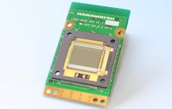
SLM for laser-based materials processing handles pulsed laser powers up to 400 GW/cm2
Because their precision is higher than conventional mechanical machining, pulsed laser machining systems are becoming widely used for processing resistant materials such as lightweight and high-strength carbon-fiber-reinforced plastics (CFRPs) and low-dielectric-constant (low-k) materials that prevent a drop in operating speed in semiconductor integrated circuits. However, several issues remain, such as the machining speed and processing throughput. Incorporating a spatial light modulator (SLM) into an industrial pulsed laser system allows irradiating diffracted multiple laser beams onto different points of a target sample simultaneously, improving the processing throughput over that for single-beam laser machining. However, so far, the output power required for this type of laser machining has been inadequate. As a result, industrial pulsed lasers with higher output power are becoming available on the market, creating a demand for SLMs that have greater resistance to high laser power levels.
Now, researchers at Hamamatsu (Hamamatsu City, Japan) have developed a liquid-crystal SLM that they say has the world’s highest pulsed-laser power capability of up to 400 GW/cm2. The reflective liquid-crystal (LC)-based SLM has a layer of LC cells sandwiched between a silicon substrate and a layer of glass; the high light-handling capability, which Hamamatsu says is 10X higher than its previous products, was achieved by improving the thin-film design of the dielectric multilayer mirrors that reflect the incident laser beam, and by redesigning the pixel electrode circuit. The SLM operates at a 1050 nm wavelength and has 1272 × 1024 pixels, an 8-bit input signal level, a 12.5 μm pitch, and a 95% aperture ratio. The Hamamatsu group notes that the SLM is viewed as an essential device for new manufacturing and fabrication techniques that use artificial intelligence (AI), such as “cyber-physical system” (CPS)-type laser-processing setups. For more information, contact [email protected].
About the Author
John Wallace
Senior Technical Editor (1998-2022)
John Wallace was with Laser Focus World for nearly 25 years, retiring in late June 2022. He obtained a bachelor's degree in mechanical engineering and physics at Rutgers University and a master's in optical engineering at the University of Rochester. Before becoming an editor, John worked as an engineer at RCA, Exxon, Eastman Kodak, and GCA Corporation.

