High-efficiency silicon-photonic outcoupling antenna is only 3.6 μm in size

Integrated photonics are usually not self-contained devices—for example, light within a photonic circuit often must be coupled out to a collecting optic, usually a fiber. To avoid having to end-fire from an integrated waveguide into an optical fiber, with the associated need to create a high-quality end facet to the waveguide at the very edge of the photonic circuit, other methods of coupling light out of a photonic circuit have been developed, with one of the most common being surface-grating antennas that diffract light out of the circuit plane for collection by an optical fiber. Numerous different designs have been created and tested, many having high efficiency. However, the gratings tend to be large, reducing the integration density.
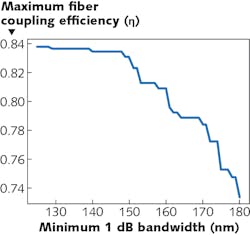
Now, a group from the National Research Council Canada (Ottawa, ON, Canada) has designed a high-diffraction-efficiency (92%) outcoupling antenna that is quite small—only 3.6 μm in its longest dimension. Fabricated on silicon-on-insulator (SOI), the device’s output can be coupled into an ultrahigh-numerical-aperture fiber (having a mode-field diameter of 3.2 μm) at a coupling efficiency of 81% (-0.9 dB) and a 1 dB bandwidth of 158 nm. The emission of the antenna is perfectly perpendicular to the plane of the SOI photonic circuit. The grating itself can either be entirely periodic, or can have a short one-step apodizing section before the periodic portion. The repeating periodic section consists of a subwavelength pillar and a partially etched L-shaped segment; the backreflection of light from the antenna into the waveguide is lower than -20 dB over the 1450–1650 nm spectral band.
The antenna outcoupler could be useful in high-density fiber-chip coupling or, because it is microscopic in size and emits vertically, for optical phased arrays. Reference: D. Malati et al., IEEE J. Sel. Top. Quantum Electron. (2020); https://doi.org/10.1109/jstqe.2020.3013532.

John Wallace | Senior Technical Editor (1998-2022)
John Wallace was with Laser Focus World for nearly 25 years, retiring in late June 2022. He obtained a bachelor's degree in mechanical engineering and physics at Rutgers University and a master's in optical engineering at the University of Rochester. Before becoming an editor, John worked as an engineer at RCA, Exxon, Eastman Kodak, and GCA Corporation.