Optical polymer waveguide backplane for high-performance computers has zero bit-error count

Optical communication technology can and will boost the speed of data-transmission in many ways: inter- and intra-datacenter, inter- and intra-computing unit, and inter- and intra-chip connections, for example. One important part of this architecture is the computer backplane, which connects printed-circuit boards together to form a computer bus. Here, optical communication will also greatly raise data transmission rates, helping to enable high-performance computers (HPCs).
A group at the Huazhong University of Science and Technology (Wuhan, China) has developed a high-speed, large-capacity, compact optical backplane based on optical polymer waveguides that use vertical-cavity surface-emitting lasers (VCSELs) emitting at 850 nm for data transmission.1 The backplane network reaches 15 Gbyte/s error-free data transmission via 8 parallel channels; in the optical backplane, the 10 Gbit/s in a channel is processed error-free by field-programmable gate-array chips.
Low transmission loss
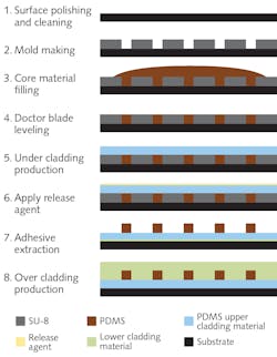
The polymer waveguide array is fabricated on a glass substrate. First, a pattern mold made of SU-8 (an epoxy-based photoresist) is created on the glass using photolithography and other methods; the polydimethylsiloxane (PDMS) waveguide material (refractive index of 1.43) in liquid form then is applied to fill the mold, leveled by a “doctor blade,” and topped by a layer of PDMS upper cladding (refractive index of 1.41). After release from the glass substrate, the assembly is flipped and the SU-8 stripped away; finally, a lower cladding (refractive index of 1.41) is applied (see figure). The resulting waveguides have a transmission loss of 0.08 dB/cm and a cross section of about 70 × 50 μm, with cladding thickness of about 150 μm.
The waveguide array is embedded in a circuit board; the light is incoupled or outcoupled via a so-called MT coupler, which routes light into or out of the waveguides via short optical-fiber sections terminated by 45° mirrors. The short fiber sections in an example MT couple are 62.5 μm multimode fibers, while the connection between a VCSEL and the MT coupler is achieved with a 50 μm multimode fiber. The insertion loss of the entire path is on the order of 2.5 dB, experimentally varying from about 1.8 to about 2.7 dB for the 8 channels.
An experimental platform was built to test the backplane: in it, a Xilinx Kintex-7 chip generated a pseudorandom bit-sequence signal modulated via a QSFP optical module transceiver; the optical signal was transmitted through the MT coupler and 4 ports of the 1 × 8 parallel polymer waveguide array, then transmitted via another MT coupler to a second QSFP, which did an optical-to-electrical conversion. Finally, bit-error-rate correction was done. For all four channels, the bit-error count was zero.
REFERENCE
1. S. Yang et al., Opt. Express (2020); https://doi.org/10.1364/oe.393039.
About the Author
John Wallace
Senior Technical Editor (1998-2022)
John Wallace was with Laser Focus World for nearly 25 years, retiring in late June 2022. He obtained a bachelor's degree in mechanical engineering and physics at Rutgers University and a master's in optical engineering at the University of Rochester. Before becoming an editor, John worked as an engineer at RCA, Exxon, Eastman Kodak, and GCA Corporation.
