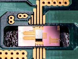
100 Gbit/s optical modulator has both photonics and electronics on CMOS silicon
Silicon photonics got its start in research labs as low-volume devices laboriously crafted using custom semiconductor fabrication processes. This is, of course, how innovation begins; the next step in silicon photonics, if things prove out initially, has been to figure out how to manufacture and use the devices more cheaply and easily. Ideally, this means moving from custom fabrication processes to CMOS-compatible—and, preferably, standard CMOS-compatible (used in computer-chip manufacture)—fabrication processes. Achieving this in any R&D project is a major step towards commercialization.
Beyond that, truly uniting both electronics and photonics on the same chip has to a large extent not yet been commercially realized, but is a goal that is widely desired. Now, researchers from the Optoelectronics Research Centre (ORC; Southampton, England) have demonstrated an all-silicon optical transmitter that can operate at 100 Gbit/s rates and beyond without the use of digital signal processing, and which is fabricated using a standard commercial CMOS process (TSMC 28 nm High-K-Metal-Gate).1 In addition, the device combines photonics and electronics as a single integrated system, including the electrical CMOS driver (see figure).
The optical modulator almost doubles the maximum data rate of current state-of-the-art devices. Optical modulators are critical components in systems serving modern information and communication technologies—not only in traditional data communication links, but also in microwave photonics and chip-scale computing networks.
Electronics need to be robust
The researchers note that to properly combine electronics and photonics on a chip, passive electrical elements such as asymmetrical transformers, peaking inductors, and termination resistors need to be low-loss over a frequency range of more than 70 GHz, even after accounting for inconsistencies introduced by variations in the CMOS process.
On the fabricated chip, the asymmetrical transformer is very small, with a size of 61 × 63 μm; the CMOS driver is connected to the two ends of a carrier depletion-based optical modulator that has a U-shaped Mach-Zehnder modulator (MZM) configuration, has a 2.47-mm-long phase-shifter section, and is designed for operation at a 1550 nm wavelength.
In a test, two independent electrical 27 − 1 pseudorandom bit sequence (PRBS) test signals were fed into a multiplexer providing signals up to 112 Gbit/s at a 0.5 V voltage swing, and the resulting output fed into the driver amplifier. The modulator output was amplified by an erbium-doped fiber amplifier (EDFA) and the signal fed into a high-speed oscilloscope. The resulting eye diagrams (a way to characterize how well high-speed modulation is being performed) showed good operation up to 100 Gbit/s with a 3 dB extinction ratio and a power efficiency of 2.03 pJ/bit.
“Our results are based upon a fully integrated electronic-photonic system, not a laboratory probed standalone silicon modulator,” says Professor Graham Reed, Deputy Director of the ORC. “In all other work to date that does not rely on digital signal processing to recover signal integrity, integration of the electronics and photonics has resulted in an inferior system performance as compared to the performance of the individual components, resulting in a maximum data rate of approximately 56 Gbit/s. At a time when most researchers around the world are striving for a system level improvement on the order of 5% to 10%, our results represent close to a 100% improvement, so we are delighted that our design philosophy is proving successful. This is why we believe these results are important, as they can change the way designers configure datacom transmission systems of the future.”
The researchers note that the bandwidth performance of their modulator prototype is already comparable to that of leading-edge lithium niobate modulators, which consume four times the power and, so far, do not have integrated drivers.
The ORC research was carried out within Southampton’s Silicon Photonics Group as part of the £6 million Engineering and Physical Sciences Research Council (EPSRC) Programme Grant Silicon Photonics for Future Systems.
REFERENCE
1. K. Li et al., Optica (2020); https://doi.org/10.1364/optica.411122.

John Wallace | Senior Technical Editor (1998-2022)
John Wallace was with Laser Focus World for nearly 25 years, retiring in late June 2022. He obtained a bachelor's degree in mechanical engineering and physics at Rutgers University and a master's in optical engineering at the University of Rochester. Before becoming an editor, John worked as an engineer at RCA, Exxon, Eastman Kodak, and GCA Corporation.
