For fused silica, combined etching and laser polishing leads to high LIDT

Damage to fused silica optics from high-power UV lasers limits the development of high-power laser systems. The traditional processing method for fused silica is grinding and chemical mechanical polishing (CMP), which is often used in fabricating photolithographic masks. This method takes a long time to produce an ultrasmooth surface and often results in surface and subsurface defects that lead to a significant reduction in the surface damage threshold of the fused silica. A research team from the Shanghai Institute of Optics and Fine Mechanics of the Chinese Academy of Sciences (Shanghai, China) has now combined chemical etching and CO2 laser polishing to process ground fused silica: chemical etching was used to open the subsurface defects of the ground fused silica, and subsequently, CO2 laser polishing was applied to reduce surface roughness. The researchers say that the combined process not only can efficiently obtain a supersmooth surface with a low surface roughness, but also can improve the damage resistance of fused silica.
In the experiment, fused silica samples 3 mm thick and 30 mm in diameter were first mechanically ground to a surface root-mean-square (RMS) roughness of 24 nm, measured with an atomic-force microscope (AFM). The researchers then subjected groups of these samples to three different processes: CMP, laser polishing (LP), and etching with hydrofluoric acid (HF) followed by LP. The results were characterized by AFM, showing RMS roughness of 0.33, 0.31, and 0.25 nm, respectively. Laser-induced damage threshold (LIDT) testing was then performed using a frequency-tripled Nd:YAG laser emitting 7.6 ns pulses at 355 nm in a single longitudinal mode. The HF-LP resulted in significantly higher LIDTs than CMP or LP alone: for example, the LIDT for 0% damage for the HF-LP sample was 29.5 J/cm2, versus that of the CMP sample at 22.2 J/cm2; the LIDT for 100% damage probability in the HF-LP sample was 47.5 J/cm2, versus 34.5 J/cm2 for the CMP sample.
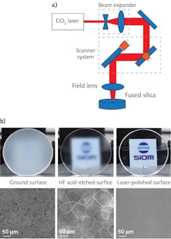
The combined HF-LP process was shown to avoid the introduction of surface and subsurface defects, including destructive defects, chemical-structure defects, and photoactive mental impurity elements, resulting in fused silica with lower surface defect densities and better damage resistance. The figure (image by SIOM) shows a schematic of a laser polishing system (a) and surface-morphology evolution during the combined process (b). Reference: Z. Cao et al., Opt. Lett. (2020); https://doi.org/10.1364/ol.409857.
About the Author
John Wallace
Senior Technical Editor (1998-2022)
John Wallace was with Laser Focus World for nearly 25 years, retiring in late June 2022. He obtained a bachelor's degree in mechanical engineering and physics at Rutgers University and a master's in optical engineering at the University of Rochester. Before becoming an editor, John worked as an engineer at RCA, Exxon, Eastman Kodak, and GCA Corporation.
