Silicon photonics gets a boost from low-profile, monolithic optical input/output coupler
Silicon photonics (SiPh) is fast becoming one of the most exciting spaces within the photonics technology area, with established multinationals, startups, and research-intensive organizations pushing custom solutions into the mainstream. Market potential is clearly articulated by organizations such as Yole Développement (Lyon, France), which recently forecast a SiPh market size of $3.9 billion by 2025, growing with a CAGR of ~40% from 2019.1 Industry analysis suggests that the widespread deployment of SiPh technology is at a tipping point and that if a few key challenges are unlocked, widespread SiPh deployment could be envisioned within a decade.2
By far, the largest current market for SiPh is in the transceiver space, both in datacom and telecom, with this trend forecast to continue over the timeframe of interest. Players established in these fields are cost-conscious, space-constrained end users, with the price per gigabyte now hovering around the $1 mark. SiPh technology is well aligned with the cost-reduction driver since much of the enabling technology can be delivered in high-volume silicon foundries. The technology also supports reduction in “real estate” for final products, as it allows the integration of the photonic components with the electronics.
Producing practical components
As with many products, however, it is not simply a case of supplying the novel component—it is a case of supplying the novel component in a usable format, and this is where the bill of materials, assembly, and test can start to play a significant part in the introduction and widespread uptake of the new SiPh technology.
Using an optical transceiver unit as an example, it has been estimated that assembly and test can contribute up to around 80% of the final cost.3 To achieve the cost targets required by the incumbent transceiver users and to encourage the other burgeoning application areas innovating in SiPh technology, assembly and test need to be significantly simplified and standardized.
With more than 50 years of concentrated worldwide development and commercialization behind it, packaging, test, and powering of the electronics-based components within SiPh technology could be considered one of the more solvable challenges for the final assembled device. Due to the commercial timelines, the packaging and distribution of light is globally less mature, especially when challenged with high-volume, scalable solutions.
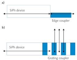
One of the key questions within the optical domain is how to couple light effectively and efficiently in and out of devices (see Fig. 1). The most-mature methods of coupling light are edge coupling (in-plane method) and grating (out-of-plane) coupling.4 In-plane coupling is attractive as it potentially offers very high coupling efficiencies, independent of polarization constraints and bandwidth. To achieve this performance, optical-quality facets are required at the device-fiber interface, constraining both the design geometries and the final packaging solution. Giving greater design freedom, the grating coupler enables light to be coupled from the optical path at almost any given point. Furthermore, it opens the potential for simpler on-wafer testing of the SiPh device, which is attractive when implementing optimized automated volume production.
Looking in detail at solutions for grating couplers, bent-fiber arrays (see Fig. 2a) are the most-mature technology offered commercially. For the end user, these present simple solutions with a variety of channel counts, pitches, and fiber types, including single-mode (SM), multimode (MM), and polarization-maintaining (PM). With volume production, the bent-fiber solution is attractive and well understood, with its basis around established V-groove array assembly technology. As “real estate” becomes a premium on the SiPh devices, fiber pitch and device height will become more important. Bent-fiber arrays are constrained by the physical long-term stressed performance of the fiber, limiting the height to approximately 5 mm or above and the fiber pitch to approximately 250 µm for high-channel-count applications. End users, however, are driving towards 127 µm pitch or lower,5 with increasingly large channel counts causing this traditional solution to become more complex to manufacture at volume.Solving both the height constraint and the pitch reduction requires the removal of the bent fiber. Using established V-groove array technology with the final fiber end facet polished to ~45° enables light turning using total internal reflection (TIR) as the guidance mechanisms (see Fig. 2b). These solutions are available from several companies specializing in connector assemblies. Because of the geometries involved, diverging light is then coupled between the fiber end facet and the SiPh device, which can introduce unwanted excess loss.
Curved surface enables 1:1 imaging
Recently, Optoscribe (Livingston, Scotland) launched OptoCplrLT, a product that enables 1:1 imaging of the optical mode within the SiPh onto the SM fiber array. By changing the 45° edge into a curved surface, additional control of the light can be implemented. These devices offer potential advantages of low form factor (<1 mm) and low coupling losses across the entire array. This product line from Optoscribe provides a scalable, monolithic lensed capability for high coupling efficiency, low footprint SiPh applications, integrating standard V-groove technology with novel, robust optical guidance methods—for example, focusing and collimating capabilities.
SiPh has the potential to transform growth areas in the electronics, photonics, and sensing markets over the next decade. To deliver on this, it is fundamental that optical designers work across the supply chain to understand how early decisions made during the basic design will impact the final product offered at volume to the market. To support take-up of SiPh across a range of industries, Optoscribe and others in the connector community are developing and shipping simple, scalable low-cost optical fiber coupling solutions into nondatacom/telecom markets.
ACKNOWLEDGEMENT
OptoCplrLT is a trademark of Optoscribe.
REFERENCES
1. See http://bit.ly/OptoscribeRef1.
2. See http://bit.ly/OptoscribeRef2.
3. See http://bit.ly/OptoscribeRef3.
4. R. Marchetti et al., Photon. Res., 7, 2 (2019).
5. D. Thomson et al., J. Opt., 18, 073003 (2016).
Tiina Delmonte | Product Line Manager, Optoscribe
Tiina Delmonte is product line manager at Optoscribe (Livingston, Scotland).

