Chalcogenide glasses have long been employed in detectors, optical fibers, and other systems utilizing the near- and mid-infrared regions. But limitations exist in other areas of the spectrum. Now, researchers have found that by making a few alterations, those confines could be overcome.
According to engineers at Duke University (Durham, NC), changing the physical shape of chalcogenide glasses can expand their use in the visible and UV ranges, leading to applications including environmental monitoring, biological imaging, and even underwater communications. The research comes after a theoretical study, in conjunction with engineers from the U.S. Army CCDC Aviation and Missile Center and the University of Brescia (Italy), in which the properties of gallium arsenide (GaAs) were examined. According to the study, a nanostructured GaAs could respond differently than bulk or thin-film nanostructures. They found that “because of the way that high-intensity optical pulses interact with the nanostructured material, very thin wires of the material lined up next to one another might create higher-order harmonic frequencies (shorter wavelengths) that could travel through them.”
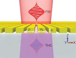
From there, the Duke researchers and a team at the U.S. Naval Research Lab applied the same idea to chalcogenide glasses. Specifically, they deposited a 300 nm thin film of arsenic trisulfide onto a glass substrate; they then used electron beam lithography and reactive ion etching to nanostructure the substrate “to produce arsenic trisulfide nanowires of 430 nm wide and 625 nm apart.” While the arsenic trisulfide absorbs light above 600 THz, the researchers note they discovered their nanowires were transmitting tiny signals at 846 THz, “which is squarely in the ultraviolet spectrum.”
According to Natalia Litchinitser, a professor of electrical and computer engineering at Duke, her team is hopeful their approach could “unlock a wide range of visible and ultraviolet applications for popular electronic material and mid-infrared photonic materials that have long been shut out of these higher frequencies.” Reference: J. Gao et al., Nat. Commun., 12, 5833 (2021); doi:10.1038/s41467-021-26094-1.

Justine Murphy | Multimedia Director, Digital Infrastructure
Justine Murphy is the multimedia director for Endeavor Business Media's Digital Infrastructure Group. She is a multiple award-winning writer and editor with more 20 years of experience in newspaper publishing as well as public relations, marketing, and communications. For nearly 10 years, she has covered all facets of the optics and photonics industry as an editor, writer, web news anchor, and podcast host for an internationally reaching magazine publishing company. Her work has earned accolades from the New England Press Association as well as the SIIA/Jesse H. Neal Awards. She received a B.A. from the Massachusetts College of Liberal Arts.
