World’s first metasurface for consumer electronics makes commercial debut
There is growing excitement around the metalens—and for good reason. Metasurfaces provide manufacturers with the ability to replace the three or four lenses (often from multiple suppliers) commonly used in complex optical systems with one single flat lens. Consider, for instance, the 3D sensing systems popular in many consumer devices such as Face ID used to open an iPhone.
“The beautiful part about metasurfaces is the ability to produce it using existing semiconductor processes,” says Metalenz (Boston, MA) CEO and co-founder Robert Devlin. “It’s moving optics into the same semiconductor foundries making the electronics, resulting in a reduction in complexity.”
Often, reducing the complexity of an optical system means compromising performance. However, the reverse has been true with the first commercial deployment for the Harvard-born startup. “We have seen improvement in overall performance, including how much light is going where it’s needed at the image sensor,” says Devlin. “And since we are moving optics into the semiconductor fab, it also serves as a means of supply chain consolidation.”
Commercial reality
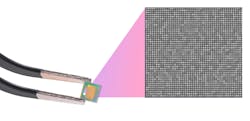
While numerous firms are working on metalenses, Metalenz is the first to announce the commercial deployment of its technology within consumer devices. The strategic partnership it announced in June 2022 with semiconductor powerhouse STMicroelectronics (ST; Geneva, Switzerland) replaces multi-element optical systems with the Metalenz optics solution (see figure).
The Metalenz offering will initially be a central component of ST’s time of flight (ToF) module known as FlightSense. The ToF offering uses the speed of light to accurately calculate proximity by measuring the time a photon takes to travel to and ultimately reflect back from a surface.
The primary offerings integrating the ST ToF module include smartphones, drones, robots, and vehicles.
Future is flat
The fact that Metalens technology provides a flat and completely planar design is what enables the use of a semiconductor fab.
“This is an important distinction because in most optical systems either the image sensor or the dot pattern projector in the Face ID, the laser source is also flat and planar,” he says. “With curved, bulky refractive lenses, you’re trying to map from a curved surface to a flat surface. And, because of that mismatch of lenses to the sensor or to the illumination source, you need all of these additional optics to correct for aberrations coming into the system.”
The flatness allows device manufacturers to eliminate the additional objects and make it just with the one single metal surface layer. As such, when integrating into modules longer term, the flat optic enables direct integration with the sensor. “You can essentially glue the lens and electronic together to make a complete optical module,” he says. “Whereas with the refractive lenses, you need them to all be separated to achieve the needed shape and curvature.”
Automotive opportunity
In addition to the consumer applications central to the relationship Metalenz has with ST, Devlin anticipates opportunities within automotive LiDAR. However, automotive LiDAR is undeniably more complicated, and more complex, than LiDAR systems present in today’s smartphones. “As the complexity adds up, it makes it harder to assemble these units with the same performance from module to module,” Devlin says.
In the consumer space, plastic refractive lenses work because the same temperature requirements do not exist. However, in the automotive space, glass lenses are crucial.
Temperature cycling is a big deal since it can cause optical properties to change. “The metasurface provides stability because we make the materials at 300-plus degrees Celsius,” he says.
Using existing semiconductor fabs means parts are cost-competitive with plastic refractive lenses, yet using solid-state materials. For the 3D sensing, Metalenz is producing lenses out of solid-state materials like silicon or silicon dioxide. “This is ideal for automotive applications because they don’t have any variation in performance as the temperature changes. There's no degradation of the optic.”
Overcoming obstacles
As with any innovative offering, the biggest challenge for a new optic technology is always gaining market acceptance. “Luckily, with this announcement that we’re making with ST Micro, we now have market acceptance,” he says. “In this year alone, our metalenses will be in millions of consumer devices.”
For Metalenz, the other hurdle was to test the mass production process to ensure the lab scale translated to semiconductor processes. “Today, we have production runs active on a real semiconductor line in a 300 mm foundry, and our technology is still achieving the needed performance.”
The next challenge, which Devlin openly welcomes, involves exploring additional applications opportunities for metasurfaces, and then appropriately expanding the offering to fit the need. “For instance, we’re looking at taking advantage of the metasurfaces’ ability to completely control the polarization of light,” he says. “While the first generation of products now has that market acceptance, we are bringing the potential of entirely new information sets to consumer scale and consumer price point for the first time.”
Bright future
“The exciting part about advancing metasurfaces is the ability to allow complex optical modules to proliferate. It allows it to go from just a few select OEMs to a price point where it can go into just about any phone,” Devlin says. “We have the initial wins, we’re doing this with existing semiconductor processes without the need for any new form of lithography or deposition, and we are leveraging existing foundries.”

Peter Fretty | Market Leader, Digital Infrastructure
Peter Fretty began his role as the Market Leader, Digital Infrastructure in September 2024. He also serves as Group Editorial Director for Laser Focus World and Vision Systems Design, and previously served as Editor in Chief of Laser Focus World from October 2021 to June 2023. Prior to that, he was Technology Editor for IndustryWeek for two years.
As a highly experienced journalist, he has regularly covered advances in manufacturing, information technology, and software. He has written thousands of feature articles, cover stories, and white papers for an assortment of trade journals, business publications, and consumer magazines.
