Photonic integrated circuits pave the way for autonomous mobility
The success of integration in electronics is about to be repeated in the optical world, paving the way toward a new era: photonic integration. Since its inception in the 1980s, silicon photonics has been a core technology. Already widely considered the next big thing in telecommunications, data centers, artificial intelligence (AI), and quantum computing, silicon photonics also shows significant potential for LiDAR for autonomous mobility.
Photonic integrated circuits (PICs) are breaking through the bottleneck of cost-effective volume manufacturability and automotive-grade reliability by placing optical components, including lasers and detectors, onto silicon chips. This technology leap shows opportunities for size and cost reduction, as well as mass production scalability. Silicon photonics offers a whole new level of system integration and should bring solid-state, frequency-modulated, continuous-wave (FMCW) LiDAR-on-Chip to fruition.
With a distinctive working principle and low laser power requirements compared to time-of-flight (ToF) LiDAR, FMCW LiDAR technology—generally regarded as an enabling sensor for autonomous mobility—is highly compatible with integrated photonic components. Co-integration of PICs and electronic ICs is enabled by system-in-package technologies such as flip chip and 3D chip stacking. This combination yields efficient and powerful photonic and electronic performance, as well as removal of fiber, which is usually cost-intensive and fragile to stringent environmental conditions faced by vehicles every day on the road.
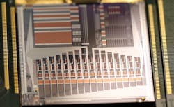
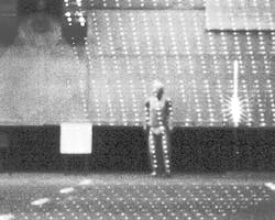
Scantinel Photonics is currently developing a FMCW optoelectronics core module (OCM) based on CMOS-compatible photonic integration platforms. The module consists of solid-state scanning PICs (see Fig. 1), with parallelization of multiple FMCW channels and Scantinel has successfully demonstrated extremely reliable scanning performance (see Fig. 2). Coupled with an advanced optical system, the module delivers outstanding scanning results while offering a compact modular approach, which can be easily adapted into any application ecosystems.How it works
The scanning PIC chip is extremely compact—less than 2 × 2 cm—and has 256 scanning lines on the solid-state, fast-scanning axis. The PIC-based scanning mechanism is essential for FMCW sensing applications and provides several advantages.
The scanning concept is the key challenge to achieve automotive FMCW LiDAR. A solid-state scanning approach without fast beam movement over the target is a prerequisite for scanning FMCW LiDAR to avoid high losses of the coherent detection system. This requires a large number of optical and electronic components, including detectors, on a very small footprint, which is enabled only by photonic integration.
Scantinel’s PIC setup allows massive parallelization to enrich pixel density, which is lacking in setups featuring only a mechanical scanner. The PIC scanning mechanism also allows users to design and customize the PIC exit pitch to have regions of interest with different resolution on the vertical field-of-view, depending on application use cases. Photonic integration significantly reduces the number of optical precision alignment steps, since many photonic components are lithographically aligned on the chip.
The solid-state PIC scanner is not only critical to fulfill and surpass automotive qualifications, it can also be fabricated at the wafer level with CMOS-compatible technology. This reduces cost, size, weight, and power consumption of a LiDAR system, so it can be scaled for high-volume autonomous mobility applications. Such implementation ensures the advantage of FMCW technology can be achieved at an attractive and competitive price point.
Wider adoption of silicon photonics
PICs bring more photonic functionality to each chip, and can also be integrated with other technologies, particularly microelectronics—using both hybrid and monolithic approaches. The trend toward higher levels of integration favors the adoption of silicon photonics for applications like LiDAR, because the integration supports a significant price- and volume-scale effect and helps accelerate LiDAR entry within the mobility space.
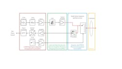
As shown in Figure 3, partitioning of FMCW LiDAR indicates a clear path to reach high integration of all required electrical, optoelectronic, and photonic sub-parts via the OCM approach. In FMCW LiDAR, all active and passive electronic functions can be integrated into one single LiDAR application-specific IC (LiDAR ASIC, red box). Standard PIC technology will be used to generate all integrated passive optical components (blue box). Light-generating and amplifying components like lasers and optical amplifiers can be integrated via a hybrid/heterogeneous approach (green box). Meanwhile, flip chip technology could be used to add the LiDAR ASIC onto the PIC carrier for ultra-integration. Additional optical components, such as collimators or mirror systems that could not be further downscaled, will be assembled with the PIC carrier using standard optic mounting technologies (yellow box).The history of FMCW radar sensors demonstrates the trend of moving from discrete components such as moving antennas and dedicated signal-processing units into highly integrated radar-on-chip concepts. The result is overwhelmingly positive: partitioning in signal-processing and control ICs, specialized radio-frequency-modules, and antenna arrays are now the state-of-the-art approach for low-cost automotive FMCW radar systems. Similarly, FMCW LiDAR partitioning into electronic, photonic/optoelectronic, and optic parts will lead to a dense system integration and considerable cost-reduction advantages for end applications.
The supply chain for the photonics industry is catching up as well. Major commercial foundries are gradually establishing new businesses toward silicon photonics with standard processes to enable low-cost and scalable manufacturability. Packaging and fabrication procedures for photonic integration are being developed to fulfill rigorous automotive-grade mechanical, electrical, and thermal requirements while minimizing the size and weight of components. And the CMOS-compatible silicon photonics approach will benefit from the silicon industry, thanks to its mature process and large-scale adoption worldwide.
The trend is crystal clear: sensors for autonomous mobility in FMCW LiDAR must be affordable, compact, highly competent, and reliable. Photonic integration will achieve the industrialization of such technology on a mass-production level.
About the Author
Michael Richter
Managing Director, Scantinel Photonics
Dr. Michael Richter is managing director at Scantinel Photonics (Ulm, Germany). He has a long-lasting senior international management background in the semiconductor, sensor, and high-tech industry. Michael holds a Doctoral and Master’s Degree in Economics.
Jin Wang
Manager - Global Business Development, Scantinel Photonics
Jin Wang is responsible for global business development and marketing at Scantinel Photonics (Ulm, Germany). He has been active in various functions in the mobility sector across U.S., China, and Germany. Jin holds a Master’s Degree in Mechanical Engineering from The University of Alabama.


