Clever optics slim down smartphone cameras
Smartphone optics started with dual cameras and evolved to as many as up to five separate lenses staring out of one smartphone. This led to ever-larger optics protruding out of the otherwise elegant, monolithic shape.
Multiple cameras mounted with a fixed baseline and angle also brought new opportunities for photographers: the ability to acquire spatial information when simultaneously shooting the same scene with different cameras. Smartphones can now create a depth map and offer new options for depth-of-field, by adjusting the focus after the shot. Blur effects can also be controlled to create special bokeh effects.
Overcoming optics protrusion
Scientists and engineers at the Fraunhofer Institute for Applied Optics and Precision Engineering IOF in Jena, Germany, collected expert know-how in the miniaturization of optics during several decades. Within their project facetVISION, they have taken on the problem of protruding smartphone optics. The more general goal of the project was to develop miniaturized imaging optics for consumer electronics, life sciences, automotive, and sensors. This project was funded by the Fraunhofer Future Foundation.
The Fraunhofer Future Foundation’s initial donation came from royalties of another famous Fraunhofer invention: the software for compressing sound files, better known as mp3-compression. Today, the foundation is guided by the concept of sustainable development. The projects of the Fraunhofer Future Foundation address the intersection between thematic areas of the United Nations Sustainable Development Goals (SDGs) and the research competencies of Fraunhofer-Gesellschaft.
The basic idea for the optical concept is to split the field of view and subsequently the optics, into two channels and to apply software stitching to derive the complete images afterward. A smaller field of view allows for smaller optical modules, eliminating the protrusion. In contrast to other approaches, the camera architecture works for any resolution and pixel size without sacrificing imaging quality.
It looks trivial to shoot two parts of an object with two separate lenses and stitch it together. But it isn’t that simple. The optical effect that occurs there, the parallax, leads to differences in images of the same object captured from slightly different positions and angles. Those differences are zero for an infinitely distant object, and the closer the object gets to the lens, the worse the parallax becomes. If one lens shoots the upper half and the other takes the lower half of an image, stitching must account for parallax effects.
The parallax error can be compensated within the stitching process with spatial information of the scene. This is why two more lenses are included to gather an in-depth map for each of the separate channels (see Fig. 2). Lenses #1 and #3 capture the upper half of the scene, and a depth map is created from the combination of their image data. The same is done for the lower half with lenses #2 and #4. The four lenses can be placed in one line. The height of their optics module is significantly smaller, about 50% of a full image-size optics module.Saving volume
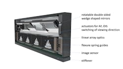
The complete camera module (see Fig. 3) uses several sophisticated technologies to achieve minimal volume, while retaining maximum performance. The prototype of the module was built using off-the-shelf hardware similar to components in other cameras, but crucial parts such as an adapted image sensor and algorithm blocks for image stitching were developed at demo-level by the partnering institute Fraunhofer IIS, Erlangen, where the mp3-audio standard was developed.
A wedge mirror bends the incoming light perpendicularly. It offers a substantial benefit – the wedge is coated on both sides and with a small rotation it switches the light path between front and back. In other words, this smartphone can use the same camera sensor for front and back photos. This not only reduces the height of the module and enables the same high resolution with depth-mapping capabilities for both camera use-cases, but also leads to module costs that aren’t higher than conventional smartphone camera solutions.
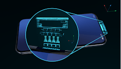
To enable an edgeless display, researchers at Fraunhofer IOF built a prototype where a camera module pops out of the side of the smartphone (see Fig. 1). This way, it leaves front and back of the smartphone completely uninterfered. Furthermore, it offers improved privacy because it becomes clearly visible when the camera is active. As an alternative to a pop-out solution, the camera might also look through the display when using in selfie mode. But imaging quality is currently still degraded in such under-the-display camera solutions.
Mechanics: Voice coil vs. twisted piezos
Autofocus and image stabilization are required to move parts of the optical system. In most smartphones, this is achieved via voice coil actuators. They need relatively high currents to generate magnetic fields, and while the currents create considerable waste heat, the magnetic fields can lead to crosstalk between different components.
A promising alternative actuator solution without voice coil motors was developed by the researchers. It relies on piezo-electric actuators. In regular smartphone camera modules, piezos are not very popular because they don’t really fit into the rather cubic modules. This looks a bit different within the facetVISION approach. The small field of view allows for a bendable optics module that is longer than regular modules, while retaining almost the same volume. Piezo-electric bending actuators for autofocus and image stabilization are much faster than voice coil actuators. They need higher voltages but much lower currents, which leads to 10 times lower energy consumption and much less heat generation and battery drain. Such actuators are available in large numbers since they have popular applications within the textile industry.
Chips and lenses
Camera technology continues to progress. Lightfield cameras appeared using extensive depth information, and other systems evolved with folded optics or multi-aperture image acquisition. The approach with a segmented field of view in combination with a folded optical path solution addresses z-height reduction, without losing image quality.
The lens system for the facetVISION module uses an off-the-shelf system with six aspheric plastic lenses per channel. In a customized system, the number of lenses could be reduced to five. A z-height reduction is achieved by making the aperture stop diameter the largest contributor to the height. Consequently, the boundary of the lenses is flattened at the bottom and top. For the prototype, the lens stacks are diced. This technology is not well suited for mass production. In that case, the desired lens shape would be generated in the injection molding process to form so called d-shaped lenses as already used in periscope-style telephoto lenses.
The individual lens stacks are placed in adapted barrels. Alignment features can be integrated in the injection-molded lenses for achieving centering tolerances of the lenses of approximately 1.2 μm with respect to each other. Given proper tolerances and alignment, all four lens modules will act similarly on temperature changes. Respective changes in the focal length can then be corrected with the autofocus drives.
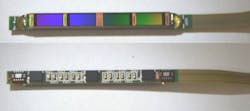
The sensor solution can be either in four separate CMOS images sensors (CIS) or in one CIS with four sensor fields. Each single sensor has to acquire a little (10%) more than half of the field of view. A conventional 20-MP sensor would be replaced by four 11-MP sensors. In the prototype, this was achieved using sensors with approximately 5,000 x 2,200 pixels. This corresponds to areas of 5.6 mm x 2.46 mm (horizontal/vertical).The benefits of multichip vs. monolithic solutions are obvious. The first solution benefits from small die areas, which go along with high yield and low cost. The second avoids the effort to integrate several dies on a common printed circuit board (PCB). Both options have been tested for the facetVISION system. For the single-chip solution shown in Figure 4, the wires located aside do not add to the z-height in the final camera module. All other components are located aside or at the rear to realize a minimum z-height.
The bottom line
Within this project, the Fraunhofer IOF researchers build prototypes to test the idea of a z-height reduction through splitting the field of view into two parts. The module can be built into a smartphone either in a fixed position or for popping out of the side (or top) of the otherwise monolithic smartphone body. It uses one camera module enabling high-resolution imaging with depth mapping capabilities for front and backside directions.
The new camera module consists of four hardware groups (see Fig. 3 top-down):
- a linear array of double-sided mirror facets, which can switch between user- and world- facing mode;
- a linear array of lens stacks integrated into a subpackage that is moved as a whole for autofocus and optical image stabilization;
- the image sensors having four pixel-matrices, in the current demo-system each of about 1-MP for a final 20-MP dual-camera output and a depth map;
- an outer packaging structure including actuators, flexure spring guides and cover glasses.
More architectures have also been developed based on other channel counts, field-of-view splitting schemes and wafer-level optics fabrication methods. These target other attractive smartphone applications such as under display optical fingerprint sensing.
The general business idea of the Fraunhofer Society is to license the technology. So the facetVISION technology is protected by a comprehensive IP-cluster that’s open for nonexclusive licensing. Royalty fees shall be collected at one point within the ecosystem, most likely from the OEMs or their tier-one suppliers, based on the number of units produced. Fraunhofer is open to mutual projects for know-how transfer and design adaptations.
REFERENCES
US2017118388 "Apparatus and method for detecting an object area“ (linear array camera with beam folding optics)
US2017264825 "Multi-aperture imaging device, imaging system and method for providing a multi-aperture imaging device“ (optical image stabilization for linear array camera with beam folding optics)
US2018241920 "Device comprising a multi-aperture imaging device, method for producing same and method for capturing a total field of view“ (linear array camera with pop-up design)
US2018198963 "Device comprising a multi-channel imaging device and method of producing same“ (linear array camera with different viewing directions)
EP2185994 “Optical navigation device” (under display optical fingerprint sensor)
About the Author
Andreas Thoss
Contributing Editor, Germany
Andreas Thoss is the Managing Director of THOSS Media (Berlin) and has many years of experience in photonics-related research, publishing, marketing, and public relations. He worked with John Wiley & Sons until 2010, when he founded THOSS Media. In 2012, he founded the scientific journal Advanced Optical Technologies. His university research focused on ultrashort and ultra-intense laser pulses, and he holds several patents.
Jacques Duparre
Jacques Duparré is a senior scientist at Fraunhofer’s Micro-optical Imaging Systems lab in Jena, Germany.
Frank Wippermann
Frank Wippermann is with the Fraunhofer Institute IOF, Albert-Einstein-Strafie, Germany. Wippermann received the degree from the University for Applied Sciences, Jena, Germany, in 1999. He worked in the field of fiber optical system design for sensing and telecommunication applications. In 2004, he joined the Fraunhofer Institute for Applied Optics and Precision Engineering (IOF), Jena, and completed his thesis on chirped microlens array configurations in 2007.,He is currently heading the Microoptical Imaging Systems Group. His main professional area is imaging optics design, and in particular, the field of wafer-level fabrication.


