The photonics revolution is well underway. Photonics started as a behind-the-scenes technology, deeply hidden in the infrastructure for undersea and fiber-optics communications—but since the start of the 21st century, there has been a steady growth in fiber-to-home, high-speed data communications, 3D sensing in cell phones and portable devices, and LiDAR solutions for autonomous-driving functions. These technologies include photonics as part of their architecture and their proliferation, particularly in consumer devices, has built momentum for the optics side of the optoelectronics industry.
To meet the needs of artificial intelligence, the importance of photonics-based processing is dramatically increasing.
As Yichen Shen, co-founder of Lightelligence puts it: “In about 2015, Moore’s law started to break down—transistors are still getting smaller, but the performance gains from the ongoing miniaturization are not as good as they used to be. What is more, the time it takes to develop the next generation of smaller devices is getting longer.”
Disruptive technology is needed—and fast.
The most obvious trend that demonstrates the necessity for greater computing power is in the escalating demand for autonomous vehicles. As auto manufacturers face increasing demand from customers for improved automation, chipmakers are turning to photonics to deliver. Initially, there was feet-off driving with cruise control, then eyes-off driving with back-up cameras and proximity detectors, and more recently hands-off driving as vehicles edge towards full autonomy.
This development requires a tremendous amount of photonics components. Photonics is required to accurately and rapidly monitor the area around you. Sensors that use photonics enable the instant transmission of data, giving vehicles the ability to alert drivers of potential hazards in their vicinity, including pedestrians or other cars.
Consumers have indicated they want more autonomous technology in their vehicles—so much so that a market research report from Fortune Business Insights forecasts the global autonomous car market will increase from $1.64 billion in 2021 to $11.03 billion by 2028.
Among the report’s highlights: “Rapid improvement in sensor-processing technologies, high-definition mapping, adaptive algorithms, and the development of infrastructure-to-vehicle and vehicle-to-vehicle communication technologies are encouraging several companies to expand their production capacities and take vehicle automation to the next level.”
Reaching that next level will require microchip makers to lean into photonic integrated circuits (PICs). What PICs can bring to automobiles, they can also deliver to data centers in terms of transfer speeds, as well as wearable devices, medical technology, and much more.
PICs can replace the conventional methods of assembling and integrating electronic and photonic components, which are outdated and expensive in terms of both capital and labor. Using PICs can lead to significant savings in cost and assembly time. But for many chipmakers, the materials that comprise most photonics devices are exotic and difficult to manufacture compared to standard silicon, a material the chip industry is heavily invested in and wants to continue to support. The materials used in photonics are used largely for LEDs, detectors, sensors, and imaging devices.
But the global photonics market is expected to grow from $722 billion to $1.2 trillion by 2028, according to a recent Skyquest Technologies market research report. This expansion is due to the burgeoning awareness that the traditional ways of the semiconductor and optoelectronics industry aren’t going to work for the long term.
What the market requires is an integration solution to “semiconductorize” photonics—producing chip-scale devices using entirely wafer-level semiconductor processing. It is only through this approach that hundreds of millions of devices can be produced, while at the same time lowering their cost, size, and power requirements.
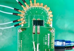
POET Technologies enhanced a traditional electrical interposer, widely used for chip-to-chip electrical communication, by adding a means for optical devices to communicate with each other and with electronic devices on a single chip.
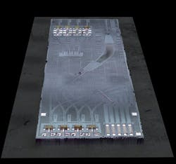
POET sandwiches optical waveguides between electrical connections to create an integrated photonics solution for the semiconductor industry. POET’s platform is based on the company’s proprietary optical interposer, which is produced solely with CMOS-compatible wafer fabrication methods, using a standard high-resistivity silicon substrate to enable high-speed communications among all the electronic and photonic components on a single chip. A wide variety of components (e.g., lasers, detectors, modulators, photodiodes, drivers, etc.) are flip-chipped and bonded onto the optical interposer. Known-good components are selected for being appropriate for specific applications. Hence, the integration is “hybrid” in character. Last year, the company announced the addition to its product designs of high-speed directly modulated lasers (DMLs) from Lumentum. It also uses continuous-wave (CW) lasers from Broadcom, adding to the best-of-breed components in its designs.
The key to POET’s optical interposer architecture and the ability to assemble and test using traditional semiconductor equipment is its low-loss waveguides. The material loss through the waveguides characterized by prism spectroscopy is less than 0.3 dB/cm and is about one order of magnitude better than typically observed in small core silicon waveguides used in other silicon photonics technologies. Moreover, the waveguides are largely athermal (dn/dT=12pm/°C) and nonbirefringent. A proprietary spot-size converter has been designed for chip facet fiber coupling and it achieves facet coupling losses of 0.25 dB.The addition of these patented waveguide layers on a conventional semiconductor wafer is critical to enabling the integration of electronics and photonics components at wafer scale. This integration has led to the world’s smallest chip-scale packaging implementation of optical engines for 100G to 1.6 Tbit/s communications. At 4.5 × 9 mm, the POET optical engine incorporates four DMLs, four high-speed photodetectors, four monitor photodiodes, and a multiplexer/de-multiplexer pair. It also reduces the overall bill of materials—an attractive feature that is especially meaningful following the supply-chain shortages of the past two years. The device is so small that a transceiver module manufacturer can fit four engines inside a standard QSFP-DD module, quadrupling data rates for a given faceplate density.
Initial customers for these first-of-their-kind integrated photonics chips and AI-ML accelerator chips built using the POET Optical Interposer include established chipmakers and startup companies. They see the hybrid-integrated optoelectronic solutions as crucial for delivering advanced performance to their clients and to end customers.
In an industry facing relentless demand for data and connectivity, photonics is the best, most viable path to achieve a future that truly moves at light speed. It’s easy to understand why the industry is predicted to be one of the fastest growing technology sectors in the coming years.
ACKNOWLEDGMENT
POET Optical Interposer is a trademark of POET Technologies.
About the Author
Suresh Venkatesan
CEO, POET Technologies
Dr. Suresh Venkatesan is CEO of POET Technologies (San Jose, CA).

