OpenLight’s CEO Adam Carter intros their PDK Sampler
Laser Focus World: What inspired your PDK Sampler?
Adam Carter: The PDK was inspired by the need to enhance familiarity with evolving process technologies and increase the accessibility of PICs. With increasing compute demands and the pace of advancements, customers can find the process of adapting new technologies to be daunting. OpenLight sought to address this challenge by providing customers with a shortcut to test individual PDK elements within their own lab and become more confident using the Tower PH18DA process.
LFW: Highlights of OpenLight’s PDK Sampler?
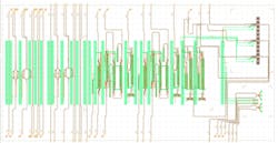
Carter: The PDK Sampler is a die-level PIC, which contains OpenLight’s heterogeneous laser, optical amplifier, 100G PAM-4 electro-absorption modulator (EAM), and other active and passive components on Tower’s PH18DA process. With the PDK Sampler, customers can validate models and test individual PDK elements within their own lab to ensure first-pass success in a PH18DA tapeout and make the most of the technology. As a result, they’re set up for success at the get-go and have a better vantage point to sample every PDK component available through our open platform.LFW: Why is now the right time for this?
Carter: The PDK Sampler not only addresses a major challenge we’ve seen among our customers, but also in the industry. Adopting new process technologies is often accompanied by a steep learning curve and can be a significant challenge, especially with recent advancements in the silicon photonics arena. This is a game-changer for anyone wanting to accelerate the use of PICs at scale within a wide variety of markets and applications.
LFW: Can you describe your partnership with Tower Semiconductor?
Carter: Tower Semiconductor is our first foundry partner for our open-foundry business model. As a close collaborator with Tower, OpenLight passed qualification and reliability tests on Tower’s PH18DA production process—providing a comprehensive library of devices to quickly jumpstart integrated PIC designs. Our latest ‘one-of-everything’ PIC is made possible through Tower.
LFW: Coolest things you’re seeing emerging within this realm right now?
Carter: There’s a recent push for platforms to double the speed per wavelength from 112G PAM-4 to 224G PAM-4. OpenLight and several other players can support this new speed-doubling capability—both optically and electrically—while significantly improving density, power per bit, and cost per bit. At the same time, co-packaged optics (CPO) is gathering steam, particularly in high-performance computing (HPC) and artificial intelligence (AI) applications.
LFW: Where do you see things heading for silicon photonics in 2023 and beyond?
Carter: In addition to faster speeds per lane and co-packaging driven by HPC and AI, heterogeneous silicon photonics is being pursued by an increasing number of companies. All of these trends will continue to accelerate the adoption of silicon photonics across a broad array of applications. OpenLight is excited to lead the charge on this front by offering a capability that enables all companies to design their own PICs—for any use case.

