Metalens controls light within the extreme ultraviolet realm
A team of researchers from Harvard University (Cambridge, MA) and Graz University of Technology (Austria) recently created the first metalens to focus beams of extreme ultraviolet (EUV). This feat opens the door to exploring microelectronics and fundamental physical processes at an attosecond level (see video).
Marcus Ossiander, a postdoctoral fellow in Federico Capasso’s group at Harvard and now working at Graz University of Technology, has a Ph.D. in attosecond physics, which requires EUV to create the shortest light pulses to observe the evolution of physical processes such as the photoelectric effect. He and colleagues struggled with a severe lack of optics for attosecond physics, because it disrupted projects or made them downright impossible.
“After I learned how to design metalenses, I had this dream a metalens might solve our problems in attosecond physics—and, it turns out, it can,” says Ossiander, who is now switching back to attosecond physics to harness these new tools.
Building an EUV metalens
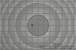
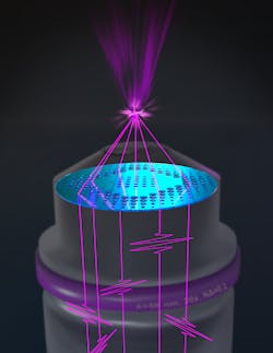
The basic design behind this work goes all the way back to the Huygens principle: treat each hole within the membrane as a tiny emitter of light. “We design the phases of these emitters so light constructively interferes in a single spot at the focal length (10 millimeters) we want to achieve,” explains Ossiander. “And we can create the design of the lens we need to manufacture hole by hole, and then fabricate the design using electron-beam lithography.”Proof of functionality was done at Graz University of Technology’s Institute of Experimental Physics with Martin Schultze’s group, which specializes in ultrashort UV light flashes. For this project, they created a light source to generate radiation to match the wavelength of the metaoptics.
Vacuum-guided EUV light
The group experienced a few “a-ha!” moments along the way, and one was “realizing we can use holes (a vacuum) in a membrane to guide EUV light with a wavelength of ~50 nm, just as people have guided visible light within silica fibers for decades,” Ossiander says. “And putting the finalized lens to the test and seeing it focus light for the first time was extremely rewarding—and also a relief after all of the work we put into it.”
One of the biggest challenges for the group was developing nanofabrication recipes. “It was difficult and took years to do, because we had to shrink the features in our lens by a factor of 5 compared to ones ‘normal’ metalenses use,” says Ossiander. “Maryna Meretska, a postdoctoral researcher in Capasso’s group at Harvard, worked hard to create our device. With the recipes we’ve developed, we can now make new optics much faster. The next challenge will be to shrink features even more to make optics for ever-shorter wavelengths.”
It’s important to note this is the only transmissive optics technology within the EUV regime that creates clean foci and images. “So far, EUV optics with large numerical apertures are either unavailable or huge, so they cost hundreds of thousands of dollars,” Ossiander points out. “Our technology allows us to shrink these optics and makes it much easier to fabricate them, which may help bring EUV microscopes into laboratories.”
Closing in on the diffraction limit
The team is now exploring how close they can get to the diffraction limit and whether it’s possible to improve the efficiency of the lenses by tweaking their designs.
“This is the first universal optics technology for EUV, so now we can start making optics like holograms,” says Ossiander. “And since these lenses enable focusing short (femtosecond to attosecond) bursts of light into tiny spots, it makes them ideal to build a microscope to better explore and understand the next generation of nanophotonics devices, such as integrated optoelectronics and plasmonic devices for energy harvesting.”
While this work may appear to be fundamental research, EUV is already being used today to create microchips for smartphones and computers—and the team now hopes the technology will help push not only the limits of fundamental research, but also reach beyond to semiconductor manufacturing.
FURTHER READING
M. Ossiander et al., Science (Apr. 6, 2023); doi:10.1126/science.adg6881.
About the Author
Sally Cole Johnson
Editor in Chief
Sally Cole Johnson, Laser Focus World’s editor in chief, is a science and technology journalist who specializes in physics and semiconductors.


