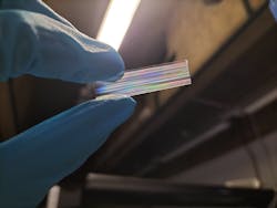
Ability to write waveguides in sapphire opens door to sapphire photonic chips
Photonic integrated circuits (PICs) require compact integration of photonics devices on a bulk substrate material, which today is primarily glass. But glass has limitations, so University of Oxford (U.K.) researchers are exploring sapphire as an alternative substrate material (see video).
Building a high-quality integrated photonics circuit in sapphire could open up numerous possibilities for applications such as communications, sensing, or quantum computing.
“The basic building block of any compact photonic circuit is a waveguide,” says Mohan Wang, a research member in the Department of Engineering Science at Oxford. “We can ‘write’ arrays of waveguides in designed patterns using laser fabrication. When we inject light into them, light propagates along the designed pathway, so we can potentially write hundreds of waveguides in sapphire to achieve very complex functions.”
Femtosecond lasers can write waveguides in sapphire
A femtosecond laser can write these waveguides inside bulk materials, because it has extremely high intensity and can be focused to a micrometer scale. “This causes nonlinear ionization inside the material in a focal volume, which results in a refractive index change,” says Wang. “From the relative movements between the femtosecond laser and our sapphire bulk material—mounted on a three-dimensional nanometer-precision stage—along a designed trajectory, we can write our designed integrated photonics on a sapphire substrate.”
A waveguide is formed by an area of higher refractive index material relative to its surrounding regions, and the most common material in integrated photonics is glass.
“Exposing glass to a femtosecond laser increases its refractive index, so it’s straightforward to write waveguides by scanning the laser along the inside of the sample,” says Wang. “But in a crystal, the laser decreases the refractive index. So instead of writing where we want the waveguide to be, we write around the outside of it to lower the surrounding refractive index. This is known as a depressed cladding waveguide, which we used in our previous work with sapphire optical fiber.”
Compared to the group’s previous work in sapphire, they’ve improved the process and reduced the optical loss of the waveguides. It enables them to now write 4-cm-long waveguides, which in turn means they can write more complex structures like a 1:2 splitter (see figure).
Once the group optimized their waveguide building block, they duplicated it multiple times. “The process control was so good they all came out the same,” says Wang. “At this point, we knew integrated sapphire photonic chips are a realistic prospect.”
Calibrating the laser writing process
A big challenge along the way, however, was the difficulty of calibrating the laser writing process.
The refractive index change “is critical for designing an optimized structure,” explains Wang. “This is especially true for crystals because they have a high refractive index and many refractive index measurements are destructive. But writing a photonics circuit requires very precise control over the laser modification profile, so it’s also desirable to do the characterization fast.”
To do it fast, the researchers write a linear array design to provide a unique output pattern. The pattern is directly related to the refractive index change and can be used as a fingerprint. “By correlating the patterns with a set of simulation results, we could identify the index modulation,” Wang says. “It enables fast and robust calibration before each fabrication run.”
Since sapphire is a very hard and resilient material, “it can survive ultrahigh temperatures up to 2000°C and high radiation,” says Julian Fells, principal investigator of the project. “These properties make it suitable for extreme environments such as aerospace, space, and power generation. It also has a very wide spectral window into the mid-infrared, where it may find medical applications. By increasing the complexity of the photonics circuits, higher-performance sensors and devices are possible.”
As the team recently shared at CLEO, they’ve demonstrated fundamental building blocks for a photonic chip and are now actively working to reduce the loss and further extend the complexity of the circuits.
FURTHER READING
M. Wang et al., “Femtosecond Laser Written Integrated Photonics on Sapphire,” paper AM2R.3, CLEO 2023 (proceedings to be published later).
About the Author
Sally Cole Johnson
Editor in Chief
Sally Cole Johnson, Laser Focus World’s editor in chief, is a science and technology journalist who specializes in physics and semiconductors.

