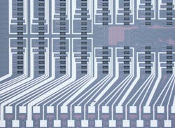
Researchers from Politecnico di Milano (Milan, Italy) and Stanford University (Stanford, CA) built a photonic neural network (PNN) chip that uses a photonic accelerator to do calculations quickly, powerfully, and efficiently (see video). The chip hosts optical waveguides connected by controllable nodes that enable a programmable photonic mesh—a grid of silicon interferometers.
“Optically, this circuit implements a fully reconfigurable multipath interferometer. From a functional viewpoint, it performs additions and multiplications directly in the optical domain,” says Francesco Morichetti, who leads the Photonic Devices Lab at Politecnico di Milano. “This means that if we feed light signals at its input ports, the output signals will be a linear combination of the inputs.”
Mathematically, it’s simply a matrix-vector multiplication—essential algebra required in computing. “Many typical computing operations are in this form, and luckily, whatever is described by a linear operator can be handled quite easily and efficiently in optics.”
The PNN chip is the result of a long-lasting collaboration that began more than five years ago between the Milano and Stanford teams.
Morichetti and fellow Milano researchers were designing programmable silicon photonic architectures, specifically advanced algorithms to automate control of these structures. At the same time, researchers at Stanford had theoretically conceptualized photonic architectures that could potentially implement sophisticated functionalities, but still required translation into a physical photonic circuit.
“Our expertise in photonics was complementary,” Morichetti says.
It’s all in the details
The photonic meshes at the core of the new PNN chip are general-purpose circuits or programmable photonic processors (see Fig. 1). To some extent, Morichetti explains, they can be considered the optical counterpart of electronic FPGAs (field-programmable gate arrays in integrated circuits), even though photonics is inherently analog.
Before PNNs, the chip technology was used in several research projects at Milano, in collaboration with Stanford. For example, they used photonic processors to generate and receive free-space optical light beams with suitable shapes to optimize transmission, communication, and sensing through semitransparent obstacles or scattering media.
“We also used a photonic mesh to unscramble, directly in the optical domain, several light beams that were mixed up after transmission through a scattering medium,” Morichetti says. “It allowed us to recover the information carried by individual beams, which has relevant implications for high-capacity transmission systems exploiting multiple optical modes.”
Neural networks must perform complex functions and adapt their behavior by examining the effects of previous actions. This training is energy- and power-intensive, but building neural networks on photonic chips paves the way for more energy-efficient computing units (see Fig. 2).
A main challenge involved in using photonics to implement efficient neural networks, however, is in the ability to exploit optics in the training of the networks. Sunil Pai, a former researcher at Stanford who is now a quantum architect at PsiQuantum, a Palo Alto, CA-based computer hardware manufacturer, says this is the most demanding part of the job.
“So far, PNNs have been used only to perform inference tasks in systems already been trained by using external computers, which substantially limits the advantage of using photonic hardware,” Pai says.
But in their work, Pai’s group at Stanford demonstrated that a PNN can be trained in situ. To this end, they’ve used an ad-hoc implementation of backpropagation algorithms. As with conventional backpropagation, the network is fed with training input data and asked to make predictions. At each iteration, the prediction error is evaluated and fed backward through the network, so the nodes of the photonic mesh are optimized to improve the prediction. Now, these procedures are done entirely via light signals for both the training data and the error data.
“This result is an important milestone because it’s proof that a PNN can be trained directly and efficiently in the optical domain,” Pai says. “And at the end of the training process, the PNN shows performance comparable to a conventional digital neural network.”
The researchers monitored the photonic chip throughout the training process by measuring the light tapped out from specific points of the mesh with a near-infrared camera. At this stage, only the linear operations of the PNN are implemented optically. This is the most computationally expensive task. “The activation function—the nonlinear operation associated with the output of each neuron—is still carried out digitally off-chip. Efficient implementation of on-chip nonlinear operations will be the next step toward fully photonic AI computing on-chip,” Pai says.
Next steps
The network training aspect is still at the proof-of-concept level, because the team’s initial results were achieved on a relatively small network. To scale the training for larger PNNs, Pai says the researchers will need more efficient control of the photonic chip. Currently, the photonic mesh is programmed using thermal actuators that are rather slow, energy-consuming, and suffer from mutual thermal crosstalk.
Solutions to implement faster and energy-saving actuators in integrated silicon photonic chips are emerging that use micro-electromechanical systems (MEMS) or electro-optical materials, which would allow the researchers to scale up the size of the PNN.
Integrated photodetectors are available in silicon photonics, as well, and can reduce the amount of light wasted in monitoring operations and improve accuracy vs. energy consumption.
“The benefits provided by photonics with respect to traditional digital processing increase when massive computing is required,” Morichetti says.
About the Author
Justine Murphy
Multimedia Director, Digital Infrastructure
Justine Murphy is the multimedia director for Endeavor Business Media's Digital Infrastructure Group. She is a multiple award-winning writer and editor with more 20 years of experience in newspaper publishing as well as public relations, marketing, and communications. For nearly 10 years, she has covered all facets of the optics and photonics industry as an editor, writer, web news anchor, and podcast host for an internationally reaching magazine publishing company. Her work has earned accolades from the New England Press Association as well as the SIIA/Jesse H. Neal Awards. She received a B.A. from the Massachusetts College of Liberal Arts.


