Stimulated Brillouin scattering enhances CMOS chip for microwave signal processing
A team of University of Sydney researchers led by Professor Ben Eggleton’s group within the School of Physics recently designed a compact microwave photonic silicon chip that combines electronic and photonic components to expand their frequency bandwidth and precisely controls information flowing through them (see video).
Combining two complementary materials—silicon and chalcogenide—enables harnessing the best of their optical properties for telecommunications. The team’s photonic chip (see Fig. 1) provides 15 GHz bandwidth of tunable frequencies with spectral resolution down to 37 MHz, which is less than 1% of its total bandwidth.
“Silicon, the material of choice for the semiconductor industry, is the basis of advanced passive circuitry, electro-optic modulation, and photodetection, while chalcogenide, a glass, provides unique nonlinear optical properties,” says Alvaro Casas Bedoya, associate director for photonic integration, who led the chip design work.
Eggleton, a physics professor, likens the simplicity of their approach to Lego building blocks, in which new materials can be integrated through advanced packaging of components using electronic or photonic chiplets. It enables integration of diverse systems on semiconductors less than 5 mm wide.
The team’s optical IC was simulated and designed in Sydney, then fabricated at IMEC in Belgium. “Our circuit contains multiple waveguides that guide photons, similar to the way metal lines within a PCB guide electrons,” says Casas Bedoya. “Our circuit was locally enhanced by a post-fabrication step at the Sydney Nanoscience Hub at the University of Sydney—the Research Prototype Foundry (RPF)—and at the Australian National University (ANU).”
Stimulated Brillouin scattering
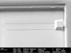
The researchers used their RFP and ANU cleanrooms and lithography to incorporate chalcogenide glass functionality into their chip. To do this, they designed an ultra-narrow silicon tip (150 nm wide) to carry the light from one material to the other one (see Fig. 2). Adding chalcogenide glass imparts a nonlinear optical effect not easily accessible with silicon and, ultimately, it enables a microwave filter that outperforms existing technologies.
“After overcoming nanofabrication challenges, we observed the nonlinear effect known as stimulated Brillouin scattering being generated from the chip,” says Casas Bedoya. “Undesired losses were incorporated as a result of a delicate post-processing step carried out in our state-of-the-art cleanrooms.”
This step arose as a necessity during the back-end-of-line (BEOL) complementary metal-oxide semiconductor (CMOS) processes at IMEC when a silica layer within the chip wasn’t removed. “Recognizing the importance of material removal, IMEC has now seamlessly included removal of this layer into its BEOL line—and it promises a substantial enhancement in the expected optical performance of our hybrid integration approach,” Casas Bedoya adds.
The success of the team’s materials integration also relied on the dedication and skills of the team members and the capabilities accessible throughout their facilities (see Fig. 3). It also reinforces the capability and expertise within their group for exquisite nanofabrication and characterization of state-of-the-art chip-based microwave photonic applications.
Advanced packaging
The researchers will “continue to enhance the filter performance and leverage opportunities arising from the additional BEOL processes mentioned earlier,” says Casas Bedoya. “We’ll also explore the integration of lasers using existing capabilities in Australia such as flip-chip packaging or wafer bonding.”
Beyond this, “it’s crucial to acknowledge the broader perspective and recognize that other materials—such as lithium niobate for modulators, and silicon nitride for low optical losses—need consideration for heterogeneous or hybrid integration,” Casas Bedoya says. “These approaches are our commitment to continue to push the boundaries of our field and to advance sophisticated heterogeneous integration and packaging techniques that are in sync with the broader semiconductor industry’s conversation currently progressing in Australia.”
The team’s efforts open the door to a new era of high-resolution radio-frequency (RF) photonic filters and other RF functionalities. These innovations feature wideband-frequency tunability to meet the requirements of future applications such as air- and space-borne RF communications payloads.
FURTHER READING
M. Garrett et al., Nat. Commun., 14, 7544 (2023); https://doi.org/10.1038/s41467-023-43404-x.
About the Author
Sally Cole Johnson
Editor in Chief
Sally Cole Johnson, Laser Focus World’s editor in chief, is a science and technology journalist who specializes in physics and semiconductors.


