PETKO DINEV
In digital cameras, the two key performance parameters are the image resolution in pixels and the speed or frame rate at which the images can be retrieved. Unfortunately, the two are interrelated—the more pixels in the image the longer it takes to retrieve them. To properly balance resolution and speed for a particular digital-camera application, a thorough technological understanding of the performance and limitations of digital image sensors is necessary.
The image sensor
The heart of a digital camera is its image sensor: the charge-coupled device (CCD). The interline transfer CCD is, essentially, an array of picture-element (light-sensitive pixel) cells that convert photons to electrons and hold the electrons until a read operation transfers them into an adjacent cell (vertical register). The read operation is analogous to emptying a water bucket into an adjacent bucket and functions as a logical shift register for the accumulated charges.
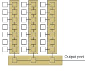
The cells in the CCD device connect in chains (see Fig. 1). Reading out an image consists first of transferring the accumulated charges from a row of active cells into adjacent masked cells that form a series of vertical shift registers. The vertical registers connect to a horizontal shift register that carries the charges to the output port of the sensor, one cell’s accumulated charge for each clock pulse. Several stages of amplifiers and analog-to-digital (A/D) converters at the output port convert that accumulated charge to a binary number.
The proper sequence of read clock signals first loads the horizontal register with one row of pixel data then shifts the row to the output port. In this way the sensor delivers its image data in a row-column format, one pixel at a time. The unmasked cells, in the meantime, have been collecting the photoelectrons that will form the next image frame.
Smaller is faster
The primary factor limiting the rate at which pixels can be clocked is the speed at which the charge transfer occurs. The resistance and capacitance of the circuits control this transfer speed and are functions of the process technology and of pixel size. As a general rule, for a given process technology, smaller pixels clock faster. Typical pixel clock rates for available CCD sensors range from 40 to 60 MHz.
The pixel clock rate, in turn, is one factor determining the frame rate that a sensor can produce. The other factor is the sensor’s resolution, or number of pixels. The more pixels a sensor has, the longer it takes to clock out the full image frame. Available sensor resolutions for the interline transfer CCD typically range from 300,000 (300k) to 16 million or megapixels (16 M).
The tradeoffs between image resolution and frame rate are not quite as simple as they look. Other factors need careful consideration, including the sensor architecture, dynamic range, and overall camera cost. These factors are interrelated, making the tradeoff analysis more complex.
Pixel size, for instance, affects more than the speed of the sensor. Smaller pixels shift faster, but have less capacity for generating and storing photoelectrons. This limitation results in a reduced dynamic range for the sensor, along with a lower signal-to-noise ratio and reduced light sensitivity.
Pixel size and optics cost
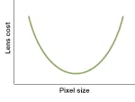
Small pixels are also more likely to capture image aberrations caused by the camera lens system. As a result, small pixel sizes impose quality constraints on the lenses, increasing camera cost. Large pixels tend to integrate out small aberrations but can lead to a larger sensor. Large sensors require the use of bigger lenses to keep the image in focus across the sensor, which also increases cost. The cost effect of pixel size choice thus forms a “bathtub” curve, indicating that there is an optimum pixel size for which optics costs are minimized (see Fig. 2).Image resolution also affects camera cost. As with the large pixels, high resolution leads to larger sensors and a need for bigger lenses. In addition, larger sensors are more likely to contain manufacturing defects, just as in other large semiconductors. These defects decrease the yield per wafer, increasing sensor cost.
Although there is no upper limit on the pixel count that a sensor can contain, the charge-transfer efficiency of the CCD cell-which measures the percentage of a cell’s charge that will transfer to the adjacent cell-becomes the limiting factor for large displays. Without a transfer efficiency very close to 100%, some charge will be lost at each stage of the shift register, resulting in the appearance of a ghost image imposed on the subsequent frame because of the residual charge.
Transfer efficiency for a CCD sensor, along with its efficiency in converting photons to electrons, is determined by the manufacturing process technology of the CCD. Each sensor vendor has its own “secret sauce” in the manufacturing of these sensors, which controls the boundary values on the cost, size, sensitivity, and speed of their sensors. Thus, the tradeoffs to be made when selecting the camera’s sensor vary from vendor to vendor and are continually evolving as technology improves.
Architecture boosts frame rate
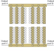
It is not just the sensor physics that need consideration, however. While higher resolution generally reduces the frame rate a sensor can achieve, the frame-rate decrease can be mitigated through sensor architecture. For example, a sensor can use multiple horizontal-shift registers, breaking the image into sections that can be clocked out simultaneously (see Fig. 3). Each such division increases the achievable frame rate, but imposes additional system costs. Each section will need its own amplifiers and A/D converter to read the pixel data. Further, these pixel-reading sections will be more expensive than usual because they require careful matching to maintain uniformity across the full image.Such multisection sensors are available in camera systems aimed at high-speed applications such as high-resolution video or the study of rocket exhaust dynamics. One manufacturer, for instance, offers an 8-megapixel camera with a 60-frame-per-second (fps) rate that uses a 16-section sensor. A 1-megapixel camera for a military application offers a 1000 fps rate and has a sensor with 64 sections.
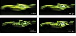
The right tradeoff between pixel size, resolution, frame rate, and system cost depends heavily on the application (see Fig. 4). Automated video inspection systems for the glass in liquid-crystal displays (LCDs) requires high resolution to detect surface defects. The camera does not have to be very fast, however, as the glass panel is difficult to move quickly. Inspecting the spacing of the glass in plasma displays, on the other hand, has a greater need for high speed than high resolution because there are thousands of spacers per display. In a typical machine-vision application, the camera speed controls the inspection station’s throughput, which affects manufacturing cost. Cell-phone manufacturing, for example, requires good resolution and high speed to quickly inspect circuit boards containing small components.Configurable cameras offer flexibility
Sometimes the right tradeoff can change. Manufacturing lines that handle a variety of products may need a camera with high resolution for one run and a camera with maximum speed for another run. Fortunately, configurable cameras are available. These cameras allow the user to configure them for a variety of resolution and speed configurations. The Imperx Model IPX-4M15L, for example, can run at 15 fps with a 4-megapixel resolution, 30 fps at 2 megapixels, or 60 fps at 1 megapixel. In a dynamic production environment where needs change, such cameras allow users to tune the inspection system to meet current needs without changing cameras.
PETKO DINEV is president of Imperx, 6421 Congress Ave., Boca Raton, FL 33487; e-mail: [email protected]; www.imperx.com.


