Large-scale monolithic photonic integrated circuits may extend the scaling benefits of Moore’s Law to optical components.
SERGE MELLE
The growth in Internet-protocol (IP) core network capacity continues to impose important scaling requirements on the underlying optical transport network used to carry this traffic. Numerous industry studies of IP network growth rates agree that a doubling of Internet traffic each year represents a sustainable natural growth rate (see Fig. 1).
FIGURE 1. Traffic projections based on aggregate monthly IP network capacity on U.S. Internet backbone networks from 1990 to 2000 indicate that between 2000 and 2010 Internet traffic is expected to increase by a factor of 1000.
This growth in IP network bandwidth has also driven the need to scale direct router-to-router connectivity to handle traffic volumes and to enable efficient multiplexing and traffic engineering to accommodate “bursty” traffic patterns inherent in the nature of IP traffic, such as time-of-day-dependent service usage spikes and service restoration requirements.
Thus, peer-to-peer router connectivity-which initially consisted of one to several digital signal level 3 (DS-3) connections at 50 Mbit/s each in the early 1990s-scaled to optical carrier level 3 (OC-3 [transmission speeds of up to 155.52 Mbit/s]) and up to OC-48 bandwidth in the late-1990s, and has continued to scale to one or more OC-192 trunks since. Today Internet service operators are introducing next-generation core IP routers having 40 Gbit/s trunk interfaces, and planning is under way toward the definition of ultra-high-data-rate Ethernet interfaces at 100 to 160 Gbit/s.
Total IP network capacity growth and the introduction of ultra-high-bandwidth IP interfaces thus poses significant challenges to operators who will seek to scale their optical transport network-which potentially will need to support up to 10 Tbit/s or more of capacity per fiber and 100 Gbit/s service interfaces between routers. Unfortunately, existing high-capacity wavelength-division-multiplexing (WDM) transport systems may be inherently limited in their ability to efficiently scale to support these requirements, and addressing the requirements involves tackling many disparate issues, including system size and density, power consumption, number of circuit packs required, intra- and interchassis fiber interconnections, spectral efficiency, and feasibility of operating faster line rates over existing fiber infrastructure.
As an example of the scaling challenge this growth presents, a typical WDM system deployed to support existing IP backbone capacity of 640 x 10 Gbit/s by 2012 would need to scale to more than 650 line cards, 14 bays, and require up to 350 intra- and interbay fiber connections, thereby significantly increasing operator costs for floor space, power, and increasing complexity for system deployment, operation, and maintenance. Clearly, new technology advances are required to make such scaling economically feasible.
PICs scale to 1.6 Tbit/s
One partial solution to this scaling challenge is to increase the line rate per wavelength, thereby reducing the number of line cards required, which would reduce the fiber-management and space challenges described above. Wavelength-division-multiplexed systems operating at line rates of 40 Gbit/s have now been field-deployed, alleviating these challenges from a technical perspective. However, industry efforts remain focused on making this option economically attractive compared to system operation at 10 Gbit/s per wavelength, such that widespread implementation of 40 Gbit/s WDM technologies is generally not expected to occur widely for several years.
While industry consensus seems to indicate that sustained development of 40 Gbit/s WDM may enable these technologies to become commercially viable, there exists significant skepticism that existing networks would support further capacity scaling of line rates, to 100 Gbit/s per wavelength, for example. This skepticism is due to several factors: significant scaling of optical impairments at such line rates, including chromatic- and polarization-mode dispersion; difficulties in implementing required optical signal-to-noise ratio and quality factor (Q) for reliable transmission over typical fiber span lengths; and the feasibility, maturity, and availability of optical and electronic components-such as p-i-n/APD detectors, transimpedance amplifiers (TIAs), modulators, and modulator drivers-that would operate at such high bit rates.
The development of large-scale, monolithic photonic integrated circuits (PICs) in indium phosphide (InP) and the advent of commercially available PIC-enabled WDM transport systems has allowed the industry to explore an alternative approach to WDM system design and associated scaling of IP core network capacity. The fundamental advance provided by photonic integration is a significant consolidation of optical components into a common substrate and device, thereby enabling many WDM channels and optical functions (including lasing, modulation, multiplexing/demultiplexing, detection, attenuation and amplification) to be implemented into a single fiber-coupled component (see Fig. 2).
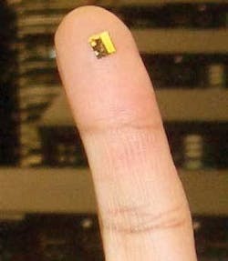
FIGURE 2. A typical photonic integrated circuit made in indium phosphide consolidates all the elements of a 10-channel WDM system operating at 10 Gbit/s per channel and has an aggregate capacity of 100 Gbit/s in a single fiber.
This consolidation creates significant flow-through benefits that can be applied to PIC-enabled WDM system design to specifically address the network capacity scaling requirements. These include enabling capacity virtualization, which decouples high-bandwidth service creation (for example, for 100 Gigabit Ethernet [100GbE] services) from line-rate operation at lower bit rates, allows for a significant reduction in intra- and intersystem fiber interconnections, reduces space and power requirements for a given system capacity, simplifies nodal system architecture, and improves system reliability and end-to-end service availability.
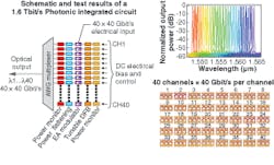
The development of PIC-enabled WDM systems appears to offer the greatest potential for enabling the continued efficient scaling of optical-transport-system density. Already, PIC-based WDM systems using 100 Gbit/s PICs have been extensively deployed in next-generation carrier networks such as Level(3) Communications (Broomfield, CO), Global Crossing (Hamilton, Bermuda), XO Communicatio ns (Reston, VA), and Broadwing (Austin, TX) to scale network capacity, provide operating efficiencies, and simplify provisioning of new high-bandwidth services. In parallel, R&D advances in PIC technology have demonstrated results of a single monolithic PIC with an aggregate capacity of 1.6 Tbit/s per PIC by operating 40 WDM channels at 40 Gbit/s each (see Fig. 3).
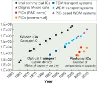
Large-scale monolithic PICs enable ever-greater consolidation of system functionality and costs compared to discrete optical devices and offer the possibility of applying the scaling benefits of Moore’s Law to optical components. As in silicon ICs, the significant level of optical-component integration and packaging consolidation enabled by monolithic integration would allow PIC technology to follow a cost-reduction curve defined by volume manufacturing efficiencies, greater functional integration, and increased device density.
Juxtaposed plots of the scaling of silicon ICs and InP PICs over time demonstrate that published PIC device performance, as well as expected commercial devices, exhibit the same level of performance scaling as defined by Moore’s Law for silicon ICs, well ahead of the device performance enhancement of discrete optical devices (see Fig. 4).
The advances enabled by new technologies such as large-scale photonic integrated circuits offer the opportunity to redefine optical transport by providing operators with the cost-effective ability to scale their next-generation IP networks and rapidly meet new and changing customer demands for broadband services, while in the process improving network flexibility and simplifying their network operations.
SERGE MELLE is vice president of technical marketing and business development at Infinera, 1322 Bordeaux Dr., Sunnyvale, CA, 94089; [email protected]; www.infinera.com.


