OPTICAL STORAGE: Miniature optical pickup has dual-suspended-film beamsplitter

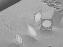
A millimeter-size short-wavelength polarizing beamsplitter devised by scientists at National Chiao Tung University (Hsin-Chu, Taiwan) could help lead to less-expensive high-capacity optical-storage devices (see figure).1 The high-extinction-ratio beamsplitter—consisting of two suspended films of silicon nitride (SiN) with a thin layer of air between them—is a lithographically fabricated component in a silicon micro-optical-bench concept pursued by the researchers.2
The precise tolerances of silicon micro-optical benches, as well as their potential for mass production, have made them candidates for optical-storage pickups. With the advent of blue-laser-based optical-storage approaches such as Blu-ray and HD-DVD, such micro-optical benches-containing lenses, gratings, beamsplitters, and MEMS-actuated mirrors-would have to handle short-wavelength light. The beamsplitter fabricated by the Taiwanese researchers overcomes the short-wavelength limitations of silicon-based optics by relying on high-quality SiN layers fabricated by low-pressure chemical-vapor deposition.
In an earlier version of the bench, the beamsplitter was a binary diffraction grating, but the operation of the improved splitter is based on Brewster-angle incidence, in which p polarization is transmitted without reflection, while s polarization is partially reflected (using two SiN films instead of one boosts the reflection).
To fabricate the beamsplitter, a silicon dioxide (SiO2) sacrificial layer was deposited on silicon, and over that two SiN layers separated by SiO2. A polysilicon frame and capping ring containing hinges and a microspring latch completed the structure. Dimples in certain layers spaced the two SiN layers apart by 0.7 µm; the SiO2 was then etched away, leaving a 500-µm clear aperture. The beamsplitter was then pried up to its vertical position with a microprobe.
In an experiment, light from a 405-nm-emitting semiconductor laser was brought to the bench via optical fiber and collimated by one of the microbench lenses, resulting in a 200-µm-diameter beam that could pass through the angled splitter. Peak reflectivity and transmissivity of the splitter were 93% and 2.8% respectively for s polarization and 0.3% and 85% for p polarization; the combined absorption and scattering loss was 14.7%. Higher-quality SiN films should improve these figures. The beamsplitter was not perfectly flat, however, but had a 12-mm radius of curvature. The group is now using silicon-on-insulator fabrication processes to improve the flatness, says Chi-Hung Lee, one of the researchers.
Lee estimates the chance of silicon-optical-bench technology being useful in optical-storage pickups as 50%. “The biggest challenge results from the limit of the optics specification,” he says. “To apply in a Blu-ray system, an objective lens with a numerical aperture of 0.85 is required. For a working distance of 400 µm between the cover layer of the disc and the objective lens, the diameter of the objective lens has to be at least 600 µm. According to our estimation, when reading the disc, the objective lens has to be precisely actuated over a 100‑µm distance horizontally and vertically to compensate for the dynamic vibration of the disc.” Combining a traditional actuating system with the microfabricated optical elements is the potential solution, notes Lee.
REFERENCES
1. C.-H. Lee et al., Optics Express 13(25) (Dec. 12, 2005).
2. Y. Chiu et al., IEEE Trans. on Magnetics 41(2) (February 2005).

John Wallace | Senior Technical Editor (1998-2022)
John Wallace was with Laser Focus World for nearly 25 years, retiring in late June 2022. He obtained a bachelor's degree in mechanical engineering and physics at Rutgers University and a master's in optical engineering at the University of Rochester. Before becoming an editor, John worked as an engineer at RCA, Exxon, Eastman Kodak, and GCA Corporation.