Filters & Coatings: Laser advances drive development of specialized optical coatings
JIANDA SHAO, KUI YI, YUANAN ZHAO, YANZHI WANG, and MEIPING ZHU
The rapid improvement of laser technology in recent years has driven the unprecedented development of optical coatings. Coatings for different laser systems have diverse specifications and requirements, including transmission/reflection values at certain wavelength range, low wavefront distortion, as well as high laser damage threshold.
To obtain the desired spectral performance, the first step is rigorous coating design. And although sophisticated commercial design software can achieve specific spectral performance, coatings for high-power laser applications must also achieve high laser-induced damage threshold (LIDT) and low coating stress.
Born as a group in an institute of the Chinese Academy of Sciences (CAS) in Changchun, China, we moved to Shanghai in 1964 as the foundation of the Shanghai Institute of Optics and Fine Mechanics (SIOM, CAS) and became the predecessor of the R&D Center for Optical Thin Film Coatings, which is now a group of Key Laboratory of Materials for High Power Laser that is tasked with evolving optical coatings—especially for high-power, ultrafast, and spaceborne laser systems.
High-power-laser coatings
Since the 1970s, we have investigated the effect of electric-field (E-field) and temperature-field distribution on the LIDT of optical coatings, demonstrating that for hafnium-oxide/silicon-dioxide (HfO2/SiO2) multilayer coatings, the lower the E-field peak value in HfO2 layers as well as placing the strongest E-field layers further from air interface, the higher the LIDT.1,2 Overcoat and undercoat layers have also been used in the coating design to improve the mechanical strength and suppress certain damage morphologies, therefore improving the LIDT.3
Total stress in a multilayer coating results from the stresses in the individual coating materials and interfaces. Since the stress of each material is different, adjusting the thickness ratio of different coating materials is a way to balance the total coating stress. So, our systematic coating design method includes the optimization of spectral performance, E-field distribution, and undercoat and overcoat layer, as well as balances stress within the coating layers.
During the coating design and fabrication process, careful layer thickness control is paramount to obtaining the desired spectral performance. Our optical monitoring approach uses witness glasses that are brought to the measuring position in a specially chosen sequence. To reduce the thickness error, some thick layers are divided into two layers and monitored by different witness glasses. With the proposed method, spectral performance close to the theoretical design can be achieved.
To improve the LIDT, it is important to understand the origin of laser damage. Defects are responsible for coating damage under laser irradiation.4 Generally speaking, decreasing the defect density and improving the laser damage resistance of the defect are effective ways to improve the LIDT, and close attention should be paid to each step involved in the fabrication process.
Using the substrate handling and cleaning process as examples, the nanoscale absorptive defects induced in the substrate polishing process may greatly degrade the LIDT of the antireflective and beamsplitter coatings, while the substrate geometrical structure may cause internal crack and E-field enhancement in the high-reflectance coating, which will consequently reduce the LIDT of coating.5,6 To reduce the defects originated from the substrate, ultrasonic cleaning and plasma ion cleaning are used to clean the substrate outside and inside the coating chamber, respectively.
In addition to substrate concerns, ejection of the coating material is also an important source of defects. By optimizing the pre-melting process of the coating materials, as well as using metallic hafnium as a starting material instead of HfO2, material ejection can be greatly decreased.
To improve the laser damage resistance of the defect, a relatively higher oxygen flow and lower deposition rate is used to benefit the coating oxidization. Recently, we proposed a co-evaporated interface to improve the multilayer interface properties and release the coating stress.7 Post-treatment processes, including laser conditioning and oxygen-plasma treatment, have also been used to enhance the LIDT.8
Optical wavefront distortion depends greatly on the surface figure of the substrate, stress control of the multilayer coating, and the environment of measurement and operation. To understand and control the stress evolution during the film deposition process, we built an in situ stress measurement system based on wafer curvature as measured by the optical deflection of two laser beams. The system allows us to de-tune coating stress by adjusting the deposition parameters.
Large-aperture coatings
Large-aperture Brewster angle polarizer coatings and mirror coatings are needed for beam steering of the SG Series Laser Facility in China, which is similar to the National Ignition Facility (NIF) in the United States and Laser Mégajoule (LMJ) in France. Plasma ion-assisted deposition (PIAD) techniques combined with traditional electron-beam deposition techniques can be used to prepare large-aperture coatings, as they can be scaled to large-aperture dimensions and tune the film stress of the optical coating while maintaining high LIDT.
Brewster angle polarizers developed by SIOM were included in the International Laser Damage Competition, held at the SPIE 2012 and 2013 Laser Damage Symposia on Optical Materials for High-Power Lasers in Boulder, CO (see www.spie.org/conferences-and-exhibitions/laser-damage). The s-polarized LIDT of our sample (41.7 J/cm2) was among the highest—just 1 J/cm2 lower than the best value (within test error). And our p-polarized LIDT of 29.8 J/cm2 was the best result of the samples submitted in 2012.
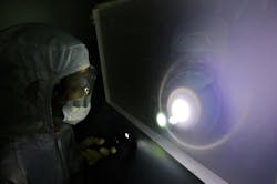
To date, we have fabricated large-aperture polarizers with p-polarized transmittance higher than 98%, s-polarized reflectance higher than 99% at 1053 nm, and can tolerate laser fluence higher than 14 J/cm2 (for 5 ns pulse width). Large-aperture polarizers up to approximately 900 mm in diameter have been fabricated for the SG II-UP laser system, as well as large-aperture transport mirrors with reflectance higher than 99.5% at 1053 nm, which can tolerate laser fluence higher than 30 J/cm2 (for 5 ns pulse width; see Fig. 1).
Ultrafast-laser coatings
Dispersion mirrors with controlled dispersion, such as chirped-mirror (CM) pairs and high-dispersion mirror (HDM) and low-dispersion mirror (LDM) varieties, are essential optics for dispersion management in ultrafast laser systems.
Offering either "negative chirp" or "positive chirp," CM pairs have been widely used for compensating the positive or negative dispersion in a particular broadband region. A combined method based on local optimization and needle optimization, using layer-thickness-modulation method as predesign, is proposed to design broadband CM pairs. Using ion-beam sputtering techniques, CM pairs with high reflectance (>99.5%) from 700 to 1400 nm and high transmittance (>99%) from 505 to 540 nm, as well as controlled group delay dispersion (GDD) of about -100 fs2, have been fabricated.
The laser-induced damage behavior of these CMs has been studied using an 800 nm, 38 fs laser. A multi-wavelength coupling ionization model can be used to illustrate the laser-induced damage behavior, which is helpful in understanding the damage mechanism under femtosecond laser irradiation.9
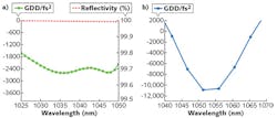
An HDM, combining the characteristics of both CM and Gires-Tournois interferometer (GTI) mirrors, has also been fabricated with a GDD of about -2500 fs2 in the wavelength range from 1030 to 1050 nm, or a GDD higher than -10000 fs2 from 1050 to 1056 nm (see Fig. 2). After reflecting eight times with the HDM with -2500 fs2 GDD, a pulse can be compressed from 1.5 ps to 150 fs.A broad-bandwidth, high-reflectance LDM is also useful to avoid introducing additional dispersion to high-power laser systems. These LDMs can achieve near-zero GDD as well as high reflectance (>99.5%) from 700 to 900 nm (45°, s-polarization), and have been successfully deployed in a 5 PW laser.10
Spaceborne-laser coatings
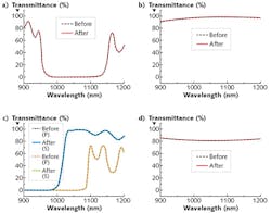
Coatings for space applications should be reliable in vacuum environments with high/low alternating temperatures, and be able to withstand long-term irradiation effects. To support the Chang'e series laser altimeters for the Chang'e lunar exploration missions, we have investigated the influences of vacuum, contamination, temperature cycling, and long-term irradiation on the performance of coatings with optimized deposition parameters for particular spaceborne environments, and have confirmed successful operation (see Fig. 3).In the past 50 years, rapid improvements have been made in laser coatings. With deepened understanding of laser-induced damage such as stress relief and the suppression of interfacial layer defects, laser coating technology is expected to achieve more progress and further evolve, promoting yet more advances in next-generation laser technology.
REFERENCES
1. Z. Fan et al., "Temperature field design of optical thin film coatings," Proc. SPIE, 2966, 362–370 (1997).
2. M. Zhu et al., Appl. Surf. Sci., 257, 15, 6884–6888 (2011).
3. M. Zhu et al., Opt. Commun., 319, 0, 75–79 (2014).
4. M. Zhou et al., Opt. Express, 17, 22, 20313–20320 (2009).
5. Y. Chai et al., Opt. Lett., 40, 16, 3731–3734 (2015).
6. Y. Chai et al., Opt. Lett., 40, 7, 1330–1333 (2015).
7. H. Xing et al., Opt. Lett., 41, 6, 1253–1256 (2016).
8. D. Zhang et al., Opt. Lett., 29, 24, 2870–2872 (2004).
9. S. Chen et al., Appl. Phys. Lett., 102, 8 (2013).
10. Y. Chu et al., Opt. Lett., 40, 21, 5011–5014 (2015).
Jianda Shao is vice director of the Shanghai Institute of Optics and Fine Mechanics (SIOM), Chinese Academy of Sciences (CAS); Kui Yi is vice director of the Key Laboratory of Materials for High Power Laser, SIOM, CAS; Yuanan Zhao is a professor, and Yanzhi Wang and Meiping Zhu are associate professors in the R&D Center for Optical Thin Film Coatings at the Key Laboratory of Materials for High Power Laser, SIOM, CAS, Shanghai, China; e-mail: [email protected]; http://english.siom.cas.cn.


