Samarium nickelate has transparent-to-opaque, blue-to-mid-IR tunability

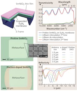
Researchers at Columbia University (New York, NY)—in collaboration with several other universities, including Harvard, Drexel, and Purdue, as well as the Brookhaven National Laboratory—have demonstrated that thin-film samarium nickelate (SmNiO3), classified as a strongly correlated perovskite material, possesses broad reflective and transmissive optical tunability from 400 nm (blue) to 17 μm (mid-infrared). Such wavelength tunability, which is the result of electron-doping-induced phase transitions, can be used to spawn a new active photonic device platform that could enable novel electro-optic modulators, programmable multilevel optical memories, smart windows for controlling sunlight, and variable-emissivity coatings for thermal camouflage and thermoregulation.
With broader-operation wavelength range, potentially faster modulation speed (there is no crystalline symmetry change during the phase transition process), and lower energy consumption (the transparent and opaque states of the material are nonvolatile), SmNiO3 improves over competing Pockels, optical Kerr-effect, electrochromic, and chalcogenide alloy devices because of its particularly strong electron-correlation effects. That is, the material is ultrasensitive to orbital occupancy of electrons and easily changes bandgap and complex optical refractive indices with electron doping/extraction at room temperature. Deposition of various thicknesses of SmNiO3 on different substrates and integration of the phase-transition material into metasurface structures resulted in several devices that demonstrated superior properties, including large and reversible tuning of optical reflectivity and transmissivity over the entire visible, near-infrared, and mid-infrared bands, and large and reversible tuning of emissivity in the mid-infrared region. Reference: Z. Li et al., Adv. Mater. online (Aug. 30, 2016); doi:10.1002/adma.201601204.

Gail Overton | Senior Editor (2004-2020)
Gail has more than 30 years of engineering, marketing, product management, and editorial experience in the photonics and optical communications industry. Before joining the staff at Laser Focus World in 2004, she held many product management and product marketing roles in the fiber-optics industry, most notably at Hughes (El Segundo, CA), GTE Labs (Waltham, MA), Corning (Corning, NY), Photon Kinetics (Beaverton, OR), and Newport Corporation (Irvine, CA). During her marketing career, Gail published articles in WDM Solutions and Sensors magazine and traveled internationally to conduct product and sales training. Gail received her BS degree in physics, with an emphasis in optics, from San Diego State University in San Diego, CA in May 1986.