Optical scattering by microscopic particles and/or surface imperfections occurs, to some degree, whenever light interacts with matter and is the primary reason that a well-collimated laser beam can be seen as it passes through air or is reflected by a mirror. Qualitatively, the amount of scattered light increases with particle density in a bulk medium and with the ‘roughness’ of a surface. Thus, the output of a low-power HeNe laser can be clearly seen in a smoke-filled room while it is virtually invisible passing through clean air. Similarly, imperfections on the surface of a laser mirror give a ‘bright spot’ at the point where an incident beam is reflected with the intensity of the scattered light decreasing with increasing surface quality.
At a more precise level, analysis of the wavelength dependence, angular intensity distribution, and polarization of the light scattered when a laser beam is reflected from a sample can provide information on the density, size, and orientation of imperfections on or near the surface. Control of surface quality and roughness is important in a wide range of manufacturing operations that include semiconductor-wafer growth, paper production, and the machining of automotive and other mechanical parts. When compared to other techniques that could be used to look at surface topology, optical scattering has the multiple advantages of high sensitivity, noncontact measurement, and potentially high throughput.
Currently, its biggest drawback is high cost. As a result, optical-scattering instruments are used in manufacturing operations in which high throughput and/or the specific performance advantages of a noncontact, optical measurement technique outweigh the expense of commercial optical-scattering instruments.
While a number of theories have been developed to quantitatively describe surface-scattering phenomena, the approximations on which they are based are rarely met in the real world. Currently available instruments are based on extensions of this basic theory to a specific type of measurement and are optimized for a specific customer base.
Total integrated scatter measures roughness
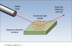
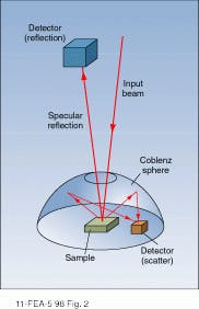
When a collimated laser beam is reflected from the polished surface of an opaque object, most of the light is specularly reflected in a well-defined beam whose angle and polarization can be calculated from classical electromagnetic theory (see Fig. 1). A small percentage of the light, however, is scattered by surface imperfections, creating a scattered intensity pattern that is determined by the polar angle of the input beam, its polarization, and the statistical properties of the surface irregularities.1While the power measured by the detector is a good approximation of the total integrated scatter in many cases, errors of interpretation have arisen when not considering the effect of the entrance aperture and the poor collection efficiency of light emitted at angles far from normal incidence. Because different instruments often have different aperture sizes, one scientist recommends that the limiting angles of the TIS collecting system be specified along with values for rms roughness.2 In addition, the highest accuracy is obtained when most of the scattered light emerges from the surface at angles near the normal.
For the assumptions made in the derivation of the equation above to be accurate, the rms roughness of the surface must be significantly less than the wavelength of the incident light. For example, the maximum roughness that can be measured by a 632-nm HeNe laser at near-normal incidence is approximately 10 nm, while a 10.6-µm source can measure values as large as 0.17 µm. The maximum surface roughness that can be measured using a particular wavelength can also be increased by increasing the angle between the incident laser beam and the surface normal. Using this technique, one 10.6-µm TIS instrument has accurately measured rms roughness values as large as 1.7 µm.
Angular resolution
While TIS systems are relatively straightforward in both design and operation, they provide no information on the surface topology. By measuring the angular distribution of the scattered light (possibly as a function of the incident beam direction), however, it is possible to better determine the detailed structure of surface imperfections. For example, if the surface of a machined metal part were grooved at regular intervals, light would be scattered from it in much the same fashion as it is from a diffraction grating, that is, it would be spread out in a fan-shaped distribution perpendicular to the groove direction.
As with a grating, the angular separation of the intensity maxima would be determined by the groove spacing while their relative intensity would provide information on their shape. Isotropic scattering produced by irregularities in both the groove profile and reflective surface would be indicated by scatter in the direction perpendicular to the fan of diffraction peaks. Thus, an angle-resolved scatter measurement performed during the machining process could provide information on both the feed rate of the tool and the way it was cutting.
More generally, imperfections on the surface of a reflective sample can be modeled as small, randomly oriented gratings, each giving rise to a fan of diffraction maxima. Describing these gratings in terms of surface spatial frequencies, it is possible to use the techniques of two-dimensional Fourier analysis to relate the measured angle-resolved scattering intensities to the distribution of surface roughness features along two orthogonal axes lying on the surface. Further information on imperfections above and below the surface can also be obtained using a polarization-sensitive measurement apparatus.
Angle-resolved techniques
Because the angle-resolved scattering-intensity distribution is a function of the incident source direction, a complete measurement of the bidirectional scattering-distribution function is a lengthy and time-consuming task that is difficult to perform outside the research laboratory. In real-world applications, prior knowledge of the surface characteristics can be used to reduce the amount of data that must be collected for process and/or quality-control applications. Most commercially available instruments are designed for specific applications in which the general features of the sample surface topology are known.
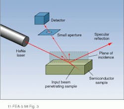
For example, one of the largest markets for surface-scattering instruments is the inspection of gallium arsenide and silicon semiconductor wafers. Instruments designed for this application typically produce a two-dimensional map of the wafer`s surface with the relative scattering intensity and/or roughness indicated by means of a color code. In an interesting modification of the basic surface-scattering instrument, VTI Inc. (Dayton, Ohio) has developed an instrument capable of mapping imperfections that lie just below the surface of a semiconductor wafer. This instrument uses a high-power HeNe laser to illuminate the sample surface and measures the angular intensity distribution of light scattered by the bulk material in a thin layer below the surface (see Fig. 3). The thickness of this layer is determined by the absorption depth of the 632-nm laser beam and ranges from 4.00 µm for silicon to 0.08 µm in zinc cadmium telluride (ZnCdTe).Using polarization techniques, the VTI instrument can map both surface and subsurface damage. In addition, the plane of incidence defined by the input beam direction and its specular reflection can be rotated through 360 with respect to the sample coordinate system. In this way, it is possible to identify directional defects or dislocations that are produced during wafer polishing or epitaxial growth.
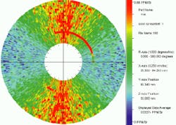
Automated scanning of the sample and instrument are controlled by a dedicated microcomputer that also converts the collected data into a usable format. In addition to two-dimensional maps of both surface and subsurface damage, the instrument can also generate a map showing directional scattering features at a series of discrete points. In this case, the data are presented as a circular, color-coded plot in which different points on the wafer surface are represented by different radii, and the angle of the plane of incidence corresponds to the polar angle. In such a plot, directional scattering features show up as bands of increased scattering intensity that stretch outward from the origin along a particular direction (see photo at top of this page).
Optical scanning techniques are particularly well-suited for the characterization of semiconductor surfaces and highly polished optical substrates because the defect size is small, and special efforts are made to keep them clean during growth and fabrication. Suitable modifications to the measurement geometry, however, can also make the technique useful for the characterization of rougher surfaces. For example, Optical Dimensions (Bozeman, MT) has developed a scattering instrument specifically designed for monitoring the surface finish of metal parts during the manufacturing process. By using a semiconductor diode laser at a large angle of incidence in combination with an angle-resolved detection scheme, this instrument is capable of measuring roughness values between 0.0025 and 1.25 µm with an accuracy of better than 2%. A dedicated software package controls the measurement process and data analysis at a maximum rate of 10 measurements per second. Data can be displayed in a number of formats including a real-time value for surface roughness.
While significantly more expensive than mechanical surface profilers and other methods of monitoring surface quality, the speed and noncontact operation of the Optical Dimensions instrument offer significant advantages in a high-volume environment. Qualitatively, these features are common to most commercial scattering instruments in the sense that they offer significant measurement advantages at higher cost. Questions of reproducibility and accuracy that once limited the use of optical-scattering instruments appear to have been resolved through an increased understanding of the measurement process.
In addition, the use of diode-laser sources and the continued development of faster electronics for data acquisition and analysis promise to favorably impact the performance and price of scattering instruments. Ultimately, the extension of scattering theory to include rougher surfaces and those contaminated with dust and other particulates will significantly increase the use of optical scattering instruments for process and quality control.
ACKNOWLEDGMENTS
The author wishes to thank Glenn Valliant of Optical Dimensions (Bozeman, MT) and Fred Orazio of VTI Inc. (Dayton, OH) for their helpful discussions during the preparation of this article.
REFERENCES
1. J. M. Bennett, "Surface Roughness Measurement," in Optical Measurement Techniques and Applications, P. K. Rastogi, ed., Artech House, Boston, MA (1997).
2. J. C. Stover, Optical Scattering: Measurement and Analysis, McGraw-Hill, New York, NY (1990).
G. J. Dixon | Contributing Editor
G. J. Dixon was a Contributing Editor for Laser Focus World.


