PHOTONIC FRONTIERS: INTEGRATED PHOTONICS: Photonic integration may boost computing performance

When Stewart Miller of Bell Labs first suggested the idea of integrated optics in 1969, the appeal of the concept came from the analogy to integrated electronic circuits, which were already a brilliant success.1 In the years that followed, integrated optics—and its descendent integrated photonics—was a perennial research topic that often seemed a solution looking for a problem. Now just such a problem has arrived, ironically because integrated electronic circuits have hit a performance wall.
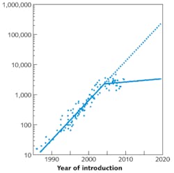
For decades, microprocessor speeds have increased as circuit elements shrank and component density increased following Moore's law. But in the mid-2000s, microprocessor clock rates stalled near 3 GHz because faster processors generated more waste heat than they could dissipate. Manufacturers got around that performance wall by designing chips with multiple cores, processors that operated in parallel so four 3-GHz chips combined to give a total processing speed of 12 GHz.
Yet the new paradigm of multicore processing can't be extended too far without major changes in software and hardware. Software that now performs operations serially must be rewritten to execute operations in parallel on chips with more than 8 or 16 cores, a National Research Council panel wrote in December.2 Integrated photonics hardware can provide that massive interconnectivity, says Samuel Fuller, CTO at Analog Devices (Norwood, MA), and chairman of the NRC panel.
Electronics, photonics, and energy
The communications capabilities of integrated photonics complement the high-performance computing capabilities of integrated electronics. Transistors excel at switching and signal processing because electrons interact strongly with each other. But the strong interactions of electrons also impair communications by generating noise and increasing attenuation in signal transmission, particularly at high frequencies. The weak interactions of photons limits optical computing, but pays off by reducing noise, attenuation, and crosstalk among optical channels. Combining the two will enhance parallel processing.
However, every computing operation generates energy, and the NRC panel warns that energy consumption and dissipation will limit performance of even highly parallel computers. "Server farms are consuming over 1.5% of the US power supply, and CMOS circuits aren't getting any more efficient in terms of energy per computation" as their speed increases, says Fuller. Massive data centers and supercomputers on the drawing boards will consume 20 MW or more of electricity, and those numbers will only go up. "If consumers expect increases of a factor of 10 to 100 [in computing speed] over the next decade, we're going to consume enormous power if we don't get more efficient."
A June 2010 white paper from the Microphotonics Center at the Massachusetts Institute of Technology (MIT; Cambridge, MA) bluntly warns that, "The projected energy consumption by Information Technology is now an unsustainable fraction of the world's electrical power generation.3" The problem is not just environmental sustainability, it's economics. "Energy now comprises 50% of the cost of ownership of IT hardware during a typical three-year life cycle," the MIT report says, adding that efforts to control energy consumption "will drive shorter product cycles and dense electronic-photonic integration."
Integrating photonic communications
"To the first order, photonics will produce much more power-efficient communications," says Fuller. Moving electrons through conductors takes energy, and the process grows worse as frequencies increase. Conductors expel electromagnetic fields, crosstalk and interference increase, and attenuation rises steeply. All three factors increase energy budgets.
Optical links have much lower attenuation and higher bandwidth, so using them between boards, between chips, and ultimately within chips promises substantial power savings. Moreover, increasing the degree of parallelism will multiply the need for communication links among processing cores. How much energy photonics can save remains unclear, but Fuller says "a factor of two or four reduction will move the ball forward." That may sound impressive, but he doesn't expect the improvement to fully offset the current doubling of electronic processing power—and energy consumption—every 18 months.
Integrating photonics links also improves a key figure of merit in high-performance computing-bandwidth density, which is measured in Gbit/s per unit cross-section area on the surface of a chip or Gbit/s per unit length on the edge of a board or chip. Optics have inherently high bandwidth density, which advanced modulation formats and wavelength-division multiplexing (WDM) can increase to levels far beyond the reach of electronics, says Lionel Kimerling of MIT's materials processing center. Integration brings photonics to smaller scales.
The shrinking of optical links
Fiber-optic links already are used commercially on backplanes of high-performance computers. The next step is to the circuit board, where Fuller is looking at integrating photonic waveguides in the board itself within a couple of years. Integration of photonics on electronic chips would follow.
Photonic integration on III-V semiconductors is already a well-established business, mostly for telecommunications, but the electronics industry wants to integrate photonics on the silicon substrates that are standard for microprocessors and most other electronic circuits. Silicon-dioxide waveguides could replace electronic conductors to distribute clock signals, which are a major power drain in purely electronic circuits. Fuller says that the easiest steps in integrating photonics with silicon are fabricating photodetectors and waveguides. Analog Devices (Norwood, MA) has already integrated silicon or germanium photodiodes and transimpedance amplifiers on silicon chips, without any additional fabrication equipment.
Integrating light sources poses a bigger challenge because silicon is a very poor emitter. So far the most successful approach has been making hybrid lasers in which III-V junctions bonded to silicon generate photons that are transferred to a waveguide in the silicon, developed by Intel Corp. (Santa Clara, CA) and the University of California at Santa Barbara (Santa Barbara, CA).
Packaging is also a major challenge because it now costs much more to transfer photons to and from chips than to transfer electronic signals. Small numbers of photonic channels can be coupled through lenses to the surface of the chip, but with no photonic technology as easy to integrate as wire bonding, Fuller calls packaging "the final frontier in which we need a cost breakthrough."
Integrating photonics and electronics
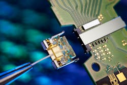
An important step on the road to integration was Intel's demonstration last year of what Mario Paniccia, director of the company's Photonics Technology Lab, last summer called in an interview "the first end-to-end silicon photonics integrated link."4
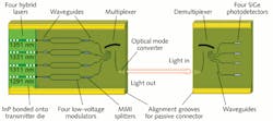
The experiment coupled an integrated four-channel coarse wavelength-division multiplexed (CWDM) transmitter through an optical fiber to an integrated receiver. The transmitter included four hybrid indium-phosphide/silicon lasers, emitting at 1291, 1311, 1331, and 1351 nm. Each fed into a separate waveguide modulator, and all four modulators fed a multiplexer which combined the four signals. An optical mode converter then coupled the combined signal into a fiber mounted into a special connector. A waveguide in the receiver chip collected the signal and delivered it to a demultiplexer, which split the four CWDM optical channels to separate silicon-germanium photodiodes. The system had a passive heat sink but no active cooling.Outlook
Optical interconnects based on integrated silicon photonics are logical extensions of technology developed for long-haul fiber transmission. The short transmission distances ease many performance constraints. Developers also are talking about potential applications in mobile electronics and automobiles as well as computers. Yet moving from the backplane to the circuit board and the chip itself also poses new challenges, particularly in cost and compatibility with silicon fabrication technology. And energy constraints are only going to get tougher, particularly for mobile devices.
Integrated photonics alone is not likely to reduce energy consumption enough to sustain the amazing rate of progress in high-performance computing. Nor is parallel computing. The NRC committee wrote that CMOS circuits will hit other limitations in a decade. We'll need a new type of electronic hardware—or, more likely, a new integration of photonics and electronics.
REFERENCES
1. S.E. Miller, "Integrated Optics – An Introduction," Bell System Technical Journal, 48, 2059–2069 (September 1969).
2. S.H. Fuller and L.I. Millett, eds., The Future of Computing Performance: Game Over or Next Level?, National Research Council (2010); http://bit.ly/eR0e0A.
3. MIT Microphotonics Center, "Scaling Limits and Energy: CTR III White Paper #1" (June 2010).
4. R. Won, "Integrating silicon photonics," Nature Photon., 5, 498–499 (August 2010).
5. A. Alduino et al., "Demonstration of a high-speed 4-channel integrated silicon photonics WDM link with hybrid silicon lasers," Optical Society of America Integrated Photonics Research Silicon and Nanophotonics, Monterey, CA, paper PDIWI5 (July 25, 2010); http://bit.ly/e8zGqi.

Jeff Hecht | Contributing Editor
Jeff Hecht is a regular contributing editor to Laser Focus World and has been covering the laser industry for 35 years. A prolific book author, Jeff's published works include “Understanding Fiber Optics,” “Understanding Lasers,” “The Laser Guidebook,” and “Beam Weapons: The Next Arms Race.” He also has written books on the histories of lasers and fiber optics, including “City of Light: The Story of Fiber Optics,” and “Beam: The Race to Make the Laser.” Find out more at jeffhecht.com.

