Microoptics: Surface functionalization -- How microoptics are changing industrial laser applications
DIRK HAUSCHILD
As laser technology matures, the question changes from "what problem can we solve with this laser?" to "what laser parameters do we need for this manufacturing process?" The designs of products ranging from consumer electronics to automobiles require new shapes and features—and these rely on laser technology.
To meet the design challenges, the laser industry must deliver appropriate systems with high durability and reasonable prices. For this task, it is microoptics that convert the laser beam from an off-the-shelf source to a custom source of heat distribution needed for a specific process.
The next major advances in laser technology will not only displace existing technologies, but also introduce new laser-enabled features. The design of modern automotive bodies already reflects that change: lightweight structures now use 3D welding processes that are only feasible with lasers. Turbine manufacturers deploy selective laser melting to create cooling channels within the blades, which is impossible with conventional casting.
Now, we have new joining opportunities, we can build up unique structures from powder, and, most importantly, we can create new surface properties. The latter becomes possible through the deposition of exactly defined amounts of heat in the shortest times. These are technologies that have left the development lab and are now in use to create great financial value. Therefore, applications exploit the unique properties of laser radiation, and it is the application that defines the laser parameters—not vice versa.
Surface modification in the semiconductor industry
To illustrate this point, lasers for flat-panel display (FPD) production represent a leading and fast-growing application (see Fig. 1). It is an application where everything is about surface modification. In this application, an excimer laser anneals amorphous silicon (a-Si) to low temperature poly-silicon (p-Si) using a small line of ultraviolet radiation that heats the silicon film on the backplane of all displays. Such systems enable large panel annealing of active-matrix organic light-emitting diode (AMOLED) backplanes for smartphones and OLED TVs, as well as polymer-based flexible display manufacturing.
Other surface modification applications are also critical. For example, structuring thin conducting layers such as indium tin oxide (ITO) on glass or polymer substrates is extremely important for many fields of consumer electronics.
Sometimes, the application concerns only certain features on the surface, while other times, it is the whole surface that changes. In these surface functionalization processes, the challenge is always the same: heat a few-microns-thick layer on the surface without harming the bulk carrier underneath.
A key element in these laser-based surface functionalization applications is the microoptics. It turns the raw laser profile into the desired shape on the workpiece, introducing an exactly defined amount of heat in a short time on the right place. In the case of Si annealing, it is a kilowatt-class excimer laser with a rectangular profile that is turned into a line measuring approximately 1 m long and <1 mm wide, with a constant energy distribution over the full length.Microoptics application development
The development of a microoptics-based laser system is determined by the process in which it is used. While it is often obvious to select a proper wavelength for an application, it may take longer to find the exact process window. That is a set of parameters where the process runs stable and efficient, even with some tolerances in material properties and laser control. Based on the process window, a laser system can be configured that meets the specifications of the process and the requirements for cost of ownership.
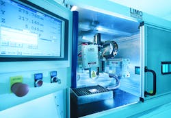
To develop such a process, we have set up a test tool at LIMO that allows intensity tuning in a laser line over six orders of magnitude. Laser diode modules with 450 W and appropriate microoptics deliver a line measuring 1 cm long and 100 μm wide. Depending on the process, the energy can be tuned from a few microjoules up to 100 J—dwell time and feed rate may be adjusted accordingly.
This helps to find the right process window and optics for processes such as annealing, heating, or melting. Once the right laser parameters are found, one can turn to scaling up the design. For example, our engineers developed processes for transparent conducting oxide (TCO) annealing. The most prominent TCO is ITO, a transparent conductor that is used for electrodes on touchscreens, OLED or LED displays, and thin film photovoltaics. Indium is an increasingly expensive material, so any savings of ITO have commercial consequences.
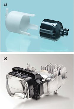
We also developed a new process for improving ITO performance on glass, where one scan increases the conductivity up to 100% without changing the glass features. This very rapid thermal processing (vRTP) activates within a 1 ms dwell time up to twice as many dopants than with regular isothermal heating, resulting in higher electron mobility and higher concentration of free carriers. After finding the right laser parameters in the lab, the process was scaled using modular lasers and optics integrated in very compact boxes (see Fig. 2).Each box produced a 300-mm-long and 300-μm-wide line using an integrated 14 kW laser diode, with some space for more power in the future. Such boxes can be combined to extend the line profile to one or more meters. In the final setup, the costs of the laser system were <$0.30 per processed square meter.
Heating in such processes is so fast that the bulk carrier is not modified. In extreme examples, laser lines can be used to meld platinum on paper without burning it. The process is completed before the heat is transferred in critical amounts. And, as opposed to conventional point-scanning technologies, it is simple to scale up.
Advanced polymer welding
The automotive industry has driven laser technology from the early days. While 20 years ago, a laser-welded car body was a statement about technology leadership, the question today is, are there any cars made without lasers?
Now, the challenge for laser technology in automotive is the great variety of materials used in manufacturing. For example, welding of plastic on plastic requires very special laser parameters. Conducting such a process with a galvo-scanner requires high heat capacity in the material, whereas a laser line needs only to be adapted to the 2D or 3D contour of the weld seam.
We have developed a process in which a 3D laser line is projected onto the workpiece to weld polymer parts, and is controlled inline. The temperature along the weld seams is observed and the laser power can be controlled accordingly, leading to perfect seams (pressure resistant to >30 bar) and passing all quality monitoring. As opposed to scanning solutions, this process requires no moving parts. Welding is performed by a customized 3D laser line contour that can be guided around the workpiece to form a full circle or other shapes (see Fig. 3).Surface modification of steel
Cutting and welding remain the biggest applications for industrial lasers, but new high-power applications arise every day. thyssenkrupp Steel Europe (TKSE; Duisburg, Germany) produces high-performance sheet metal for the automotive industry. Such material is required to possess extreme properties: it should be very stiff to enable weight reductions in the car body without compromising stability, offer plasticity for forming processes such as deep-drawing, and withstand corrosion.
A German research consortium led by TKSE developed a process to modify the surface of steel strip materials (the OSLO project). With feed speeds more than 50 m/min and band sizes beyond 300 mm, extreme high powers were required to modify the steel surface on-the-fly. LIMO developed special microoptics that transformed the beam of a 15 kW laser diode system into a 300 × 0.05 mm laser line.
The short-time melting changes the crystalline structure of the metal surface and leads not only to much improved corrosion resistance, but also to a very pleasant appearance.
This is a typical case of surface functionalization where advanced material science meets advanced laser optics. With a similar process, the Ni coatings on some bearings are hardened, leading to 3X longer durability.
Dirk Hauschild is chief marketing officer at LIMO, Dortmund, Germany; e-mail: [email protected]; www.limo.de/en.


