Multispectral Filters: Filter-array technology to bring spectroscopy to smartphones
STEVE SAXE
Every material in the universe has its own unique optical spectral signature. It is observable by shining a known light at the material and looking at the reflection; the spectrum of light coming back includes information about its material composition. Color is one aspect of such information, but human vision is limited to the wavelength range of about 400 to 700 nm (violet through red).
This range encompasses an array of colors, and just beyond it lies the shortwave near-infrared (SW-NIR), which spans from about 700 to 1100 nm. The SW-NIR is steeped in information about the material composition of the world.
Coincidentally, inexpensive and ubiquitous silicon photodetectors are sensitive to SW-NIR light, and provide the opportunity to bring consumers invisible information about the world. The key challenges are cost and size, and technology advances will soon be able to meet these and provide invisible and important information to your smartphone.
Molecular spectroscopy is the study of light's interaction with molecular vibrations, which for most common materials have fundamental frequencies that lie in the IR region of the electromagnetic spectrum, from approximately 3 to 50 μm in wavelength. In its simplest form, one illuminates the material with a known light source, analyzes the spectral content of the reflected or transmitted light, compares the measured spectrum to a database of known materials, and from that predicts the composition.
The most precise and detailed measurements can be made directly in the IR, but overtones or harmonics of those frequencies can be observed at shorter wavelengths. Near-infrared spectroscopy (NIRS) over the range of approximately 900 to 1700 nm is a well-established field of academic study that long ago crossed over into the industrial world. Historically, based on benchtop instruments, NIRS is a contributor to fields as diverse as agriculture, food and feed processing, pharmaceutical manufacturing, oil and gas production, and materials processing.
Silicon-detector-based spectroscopy is a younger discipline, but one uniquely suited to the stringent cost and size requirements of consumer devices. Silicon photodetectors and imagers have enjoyed the benefit of tremendous technical innovation in the last decade. One need only look at the last 10 years of digital-camera technology to appreciate the innovations that have brought near-professional image quality to smartphone cameras.
Many of the innovations have been in image processing and software, but silicon imager chips have also enjoyed spectacular advances that position them ideally for spectral sensing. Specifically, the advent of backside-illuminated imagers (BSIs) has increased useful light-collecting area to 100% from the 25% typical of front-illuminated imagers. Leading-edge imager makers are now offering specialized, hybrid CCD-CMOS imagers that exploit the light-collecting efficiency and charge-conserving properties of CCDs with the on-chip processing power of CMOS. The hybrid architecture also enables a deeper CCD collection well that enhances NIR sensitivity and makes imagers even better suited to spectroscopy outside the visible spectrum.
To make a spectral sensor, some means of separating wavelength must be added to an imager. An array of bandpass filters in close proximity to the imager has the advantage of using almost no additional space. This method has been used in similar forms on NASA spacecraft, including the New Horizons mission to Pluto that mapped the dwarf planet's methane and water ice.1
On a more modest scale, various companies are introducing bandpass-filter arrays either deposited directly on an imager or deposited on glass and bonded to the imager. One of the fundamental challenges in this approach is economic—for a 64-channel sensor, for example, the process might require 64 individual coating and patterning steps to create the array. Since each coating step involves the vacuum deposition of a precision thin-film filter, this number of cycles leads to scalability issues and manufacturing costs far above market requirements.
Binary multispectral filter technology
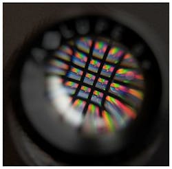
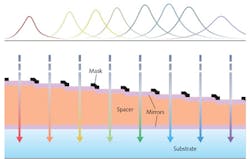
Viavi has recently developed a method of economically fabricating a numerically large array of bandpass filters that suits this application. It uses a binary scheme to incrementally fabricate the variable-thickness spacer layer in a single-cavity Fabry-Perot filter, known as binary multispectral (BMS) filter technology. In this method, a first mirror and first spacer (of thickness d, for example) are deposited on the substrate, either glass or a silicon wafer of imagers. Then, a series of patterned, incrementally thinner spacer layers are deposited, each half the thickness of the one preceding it, in the form of d/2, d/4, d/8, and so on. Finally, the second mirror and any blocking layers are added to complete the structure (see Fig. 2).Using this manufacturing-efficient method, an array of 64 bandpass filters (see Fig. 1) can be fabricated with as few as eight coating-patterning cycles. This brings potential high-volume manufacturing cost within the range of the smartphone bill of materials.
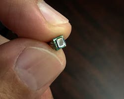
The resulting sensor need not be any bigger than the imager itself, if the micron-thin optical filters are deposited directly on the imager wafer. If deposited on glass and bonded, the overall chip thickness would increase by the substrate thickness, as little as 200 μm. Figure 3 shows a prototype sensor mounted on a small printed circuit board.Many common materials such as water, sugar, aspirin, and caffeine have readily detected optical signatures in the silicon-detector range. This opens up the potential for a smartphone sensor that is able to measure, for example, the sweetness of fruit in the grocery store, the authenticity or purity of milk powder, or a weekend warrior's level of hydration following a strenuous workout.
The integration of spectrometers into smartphones will be a major technology disrupter. Consumers will soon be able to perform a variety of scientific measurements on their own using this new feature to obtain insights on the material composition of the world around them.
REFERENCE
1. K. Hendrix, "Spectral imager maps composition of Pluto" – see https://goo.gl/Z9xxfT.
Steve Saxe is product line manager at Viavi Solutions, Milpitas, CA (formerly JDS Uniphase); e-mail: [email protected]; www.viavisolutions.com.


