High-efficiency broadband IR absorbers can serve not only to reduce stray light in IR optical systems, but also to collect radiant energy from engines, power plants, or factories that could potentially be converted to electrical power. Such absorbers are a focus of research, as evidenced by NASA’s recent announcement of a carbon-nanotube-based IR-absorbing surface and the revelation that independent researcher Robert Crowley had invented a similar nanotube-based surface more than a decade earlier.
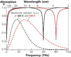
A different take on the broadband IR absorber, this one based on dielectric and metal-film multilayers, has been designed by researchers at the University of Maryland (College Park, MD) and Concord University (Athens, WV). Although only theoretical at this point, the surface promises wideband IR absorption of greater than 99% of 300 K and 500 K blackbody spectra.
A representative film structure contains 50 pairs of alternating layers of barium fluoride (BaF2) and nickel chromium (NiCr). As the dielectric, BaF2 is transparent across a broad swath of IR; as the metal film, NiCr does the absorbing. For the two examples shown, thicknesses of the BaF2 and NiCr layers are 1.34 μm and 0.18 nm, respectively (red curve), and 1.8 μm and 0.18 nm, respectively (black curve). Both structures also have a single-layer dielectric antireflection (AR) coating. The researchers are investigating a nanopatterned AR coating to tune the effective permittivity. Contact Timothy Corridan at [email protected].

John Wallace | Senior Technical Editor (1998-2022)
John Wallace was with Laser Focus World for nearly 25 years, retiring in late June 2022. He obtained a bachelor's degree in mechanical engineering and physics at Rutgers University and a master's in optical engineering at the University of Rochester. Before becoming an editor, John worked as an engineer at RCA, Exxon, Eastman Kodak, and GCA Corporation.
