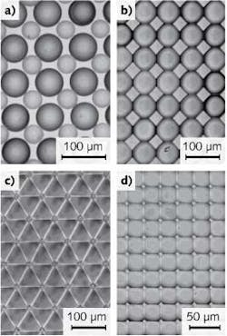
Polymer micro-optical elements or microlens arrays are typically fabricated using photoresist reflow, photolithography, and LIGA methods that require expensive masks and complex processing steps, or by maskless inkjet and self-assembly processes that limit lens quality. And while laser-direct-writing processes such as two-photon-polymerization (TPP) produce high-quality arrays, the point-by-point fabrication process is extremely slow. Researchers at Xi’an Jiaotong University (Xi’an, China), however, have created a modified laser-direct-writing process that rapidly creates high-quality glass microlens masters that can be used to replicate polymer arrays.
In the process, an 800 nm ultrafast laser delivers intensity- and time-controlled, carefully arranged, individual pulses to a glass slide that is then subjected to wet-etch processing. The laser pulses change the physical and chemical properties of the glass in the focal spots, and the wet-etch processing that follows carves out a unique microlens array pattern. An 80-μm-diameter glass mold with more than 16,000 concave structures can be fabricated in less than three hours, improving significantly on TPP processing and enabling a variety of different glass “master” shapes such as circular, rectangular, diamond, and octagonal designs. Contact Feng Chen at [email protected].
About the Author

Gail Overton
Senior Editor (2004-2020)
Gail has more than 30 years of engineering, marketing, product management, and editorial experience in the photonics and optical communications industry. Before joining the staff at Laser Focus World in 2004, she held many product management and product marketing roles in the fiber-optics industry, most notably at Hughes (El Segundo, CA), GTE Labs (Waltham, MA), Corning (Corning, NY), Photon Kinetics (Beaverton, OR), and Newport Corporation (Irvine, CA). During her marketing career, Gail published articles in WDM Solutions and Sensors magazine and traveled internationally to conduct product and sales training. Gail received her BS degree in physics, with an emphasis in optics, from San Diego State University in San Diego, CA in May 1986.
