When the ultrathin metallic needle used in an atomic-force microscope is exposed to a focused beam of light, the radiation acts as a radio wave. The needle interacts with the optical field as if it were an antenna: light polarized parallel to the needle axis makes the electrons in the needle oscillate and re-emit in a fashion like a Hertzian dipole. If the tip of the needle is in close proximity to a sample surface, the optical-field pattern evolving between tip and surface is characterized by a strong optical near-field interaction (Fig. 1). The small tip diameter (about 20 nm) of a scattering-type scanning near-field optical microscope (s-SNOM) allows mapping at a resolution far better than the diffraction limit. Researchers at the Max Planck Institut für Biochemie (Martinsried, Germany) are using this sort of instrument for structuring as well as for examining surfaces.
The dielectric functions of the s-SNOM tip and the surface region under examination both influence the light scattering. The effective polarizability (which arises from both dielectric functions) is inversely proportional to the third power of the tip-to-surface distance, the dielectric function of the surface can be conveniently traced by modulating the needle-surface distance sinusoidally—the so-called “tapping mode”—while analyzing the scattered light by extracting its content at the harmonics of the modulation frequency. In this way, strong but unvarying contributions due to geometric scattering by the tip and the surface are eliminated, and the interaction-induced part of the scattered light prevails because of its strongly nonlinear distance dependence. This technique allows the researchers to achieve both amplitude- and phase-sensitive detection, in the latter case with respect to the incident or a reference wave.1
Especially in the IR, crystals show interesting narrowband identifying s-SNOM resonances close to the longitudinal phonon frequency. Hence, IR s-SNOM can map IR-sensitive surface parameters and their variation at nanoscale resolution, in addition to recording the topographic information by the usual atomic-force microscopy.
For example, a silicon carbide (SiC) crystal surface was scanned with IR light tuned to a phonon resonance of that crystal (see Laser Focus World, November 2002, p.32). The research showed that phonon-enhanced near-field coupling is extremely sensitive to the chemical and structural composition of polar samples; application was expected in nanoscale nondestructive material analysis and in high-density durable optical-data storage.
Eying high-density IR data storage
Now, the researchers at the Max Planck Institute have succeeded in controlled nanoscale structuring of a SiC surface with respect to its phonon polariton properties.2 The technique is a first step toward demonstrating the possibility of high-density IR data storage and the fabrication of nanoscale IR circuits. Because phonon resonance is tightly coupled to the crystalline structure, and hence the scattered IR light, it sometimes almost disappears—for example, if the crystal structure is transformed to the amorphous state. Hence, controlled spatial modulation of the crystalline structure paves the way for data storage and IR optical readout.
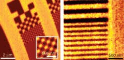
Amorphization of SiC crystals was obtained by direct-writing implantation of beryliium or gallium ions at high local resolution. In this way, checkerboard patterns were prepared with alternating “white” and “black” squares, providing high phonon-resonant signals and very low signals, respectively. For example, using gallium, different checkerboard squares of individual side lengths down to 200 nm were fabricated—a resolution of λ/50 with respect to the IR-laser readout wavelength of about 10 µm (see Fig. 2).Such patterned surfaces could be used for confining and guiding surface-phonon polaritons in nanoscale devices, or to create materials with a negative index of refraction that would form the basis of optically perfect lenses. For data storage, ion implantation could be localized to spots of about 10-nm diameter, resulting in storage densities of up to a terabyte per square centimeter. Using ion beams to write ordinary data on an ordinary compact disk may not be practical; however, for storing unique data of cultural importance with long-term requirements, it may be worth further investigation.
When tunable IR lasers or quantum-cascade lasers become more widely available, more applications of s-SNOMs will become possible, such as identifying the chemical and structural composition of many materials by their mid-IR spectra, as well as direct visualization of Cooper-pair breaking, plasmon-phonon coupling, and cyclotron resonance in solid-state materials.
REFERENCES
- F. Keilmann and R. Hillenbrand, Phil. Trans. R. Soc. London A 362, 787 (2004).
- N. Ocelic and R. Hillenbrand, Nature Materials 3 606 (2004).
Uwe Brinkmann | Contributing Editor, Germany
Uwe Brinkmann was Contributing Editor, Germany, for Laser Focus World.

