HUBERT KOSTAL and JIM WANG
Individual optical functions are most often performed by discrete optical devices that are manufactured using distinct, independently optimized manufacturing processes. Waveplates, for instance, can be precisely ground pieces of quartz or polymer thin films sandwiched between two glass plates; a polarization beamsplitter can be either a birefringent crystal (grown and then diced and polished) or a polarization beamsplitting cube (constructed from optical-glass prisms and thin-film coatings). Polarizers are either truncated polarization beamsplitters (one beam path going unused) or a thin film; wavelength-selective filters are constructed from multiple thin-film layers. Such divergent manufacturing methods can be highly optimized and low in cost for the single product for which they are applicable. Fabrication of optical devices by different manufacturing techniques, however, ultimately results in missed opportunities to achieve next-level economies of scale.
To achieve large reductions in optical-device manufacturing costs, one can look to approaches that provide both a platform technology for achieving multiple optical functions and a manufacturing method that allows for low-cost volume production. A class of optical components, nano-optic devices use the fine-scale structuring of materials at a molecular level to create useful optical properties.
Because nano-optic devices are manufactured on a wafer scale using a synthesis of semiconductor, printing, and thin-film- manufacturing methods, two benefits are realized. First, the same manufacturing method and production line can be used to manufacture a broad range of optical devices—polarizers, waveplates, filters, lenses, and so on—that would ordinarily require different production facilities. This provides the potential for breakthrough economies of scale. Second, because of the generality of the production methods used, the fabrication of nano-optics can be integrated with other wafer-based optical-fabrication technologies, allowing the direct integration of optical functionality, which eliminates manual assembly and reduces end-to-end manufacturing and component costs.
Nanostructure-based platform architecture
Over the past 20 years, research has shown that very fine subwavelength-scaled structures formed in appropriate materials can be used to realize a broad range of both common and uncommon optical effects. The most common structures used are one-dimensional grating structures with a pitch of approximately one-tenth to one-third the wavelength of the incident light and with submicron thickness. Fabricated in the right material, such a grating structure can be placed in the beam path to create effects as diverse as polarization beamsplitting, phase retardance, and wavelength-selective filtering. More-complex nanostructures such as meshes, shaped pillars, rings, and waveguide structures can be used to create additional filtering, lens, beam steering, and beam scattering (for example, antireflective) functions. The class of optical devices that are built based on these subwavelength-scale nanostructures can be referred to as nano-optics.
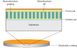
A complete model of a nano-optic device combines several elements (see Fig. 1). A nanoscale structure provides the core optical function as determined by the material used, the structural shape, and the surrounding layers and materials. An interstructure fill material modulates the nanostructure optical function and can often be chosen to provide structural robustness. A thin-film top layer provides an antireflection coating but can also be used for index matching; it also provides a protective top surface. A thin-film sublayer beneath the nanostructure usually provides an antireflection coating at the nanostructure substrate boundary and additionally provides a precise boundary between the nanostructure and the substrate. The substrate itself can simply be an optically transparent host surface for the nanostructure subassembly or it can be chosen for optical properties complementary to the nanostructure. A far-side coating can simply be an antireflection or index-matching coating, a thin-film device, or even another nanostructure.
Wafer-based manufacturing
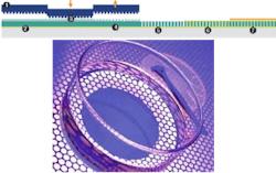
The generic nano-optic design supports a manufacturing process with highly repeatable steps and sufficient flexibility to adapt to manufacturing variability in the design to maximize throughput and yield. The nanopattern-transfer manufacturing process used to produce nano-optic devices consists of a combination of printing-like thin-film deposition and semiconductor-like processing steps (see Fig. 2).First, a complement, or negative, of the desired nanostructure pattern is etched or otherwise created in a master plate. This will be used as the guide for subsequent pattern transfer in the manufacturing operation. This is a key element of the manufacturing operation as it allows nanoscale structures to be patterned rapidly by mechanical means with high fidelity because it acts as a design-capture mechanism that allows nanostructure designs to be preserved for future manufacturing runs and it allows complex multistep designs to be constructed only once (rather than for every production wafer) and then captured or frozen. This is only done once for each nanopattern desired. The same nanopattern can be used for multiple nano-optic devices. Note that while we refer to using the "master" plate in the production steps, in practice it is a duplicate or clone of the master that is used, allowing for protection and archiving of the original.
Next, a substrate is prepared, generically consisting of an optical substrate with thin-film coatings on each side, a layer of target material for the nanostructure on one side, and a layer of pliable polymer resist on top of that. The substrate is usually a 100-, 150-, or 200-mm-diameter wafer, but other sizes and shapes are also usable.
The master plate is brought in contact with the polymer resist under appropriate process conditions. For efficiency, the master is usually identical in size to the substrate, but this is not a requirement. Process conditions are such that the polymer resist adapts to the shape in the master plate. A curing operation then sets the polymer, after which the master is separated from the substrate, leaving the desired pattern remaining in the polymer-resist layer.
Reactive-ion etching is used to transfer the pattern to the target material (which can be the substrate itself) by uniformly etching away the resist. The internanostructure space, or trench, is filled using various deposition methods. Then the top-layer thin-film coating is applied. The final wafer output is tested for uniformity and optical properties and then diced into appropriately sized nano-optic chips.
Masters are long-lasting
One 100-mm-diameter wafer has sufficient area to produce more than 7000 mm2 of optical chips, post-dicing. By using the same master repeatedly, high-volume runs of hundreds of thousands of optical chips can be performed in relatively short order. By changing the master used, the same manufacturing line can produce a broad array of optical devices, creating a cross-product economy of scale not generally available in the production of optical components.
Integrated optical devices are manufactured through the same process. Allowing spatial variations in patterns across the mold—most commonly as pixel-like regions—creates horizontal regions of differing optical function on the same nano-optic chip. Running a wafer through the nano-imprint manufacturing process more than once allows a layering of nano-optic structures and functions. Each layer can either be simple (one uniform pattern) or complex (pixilated patterns). Integrated devices can also be created by combining the nanostructure with complex and optical functional substrates, such as epitaxially grown crystals, liquid-crystal layers, MEMS (microelectromechanical systems) devices, and others, allowing the production of highly compact optical components.
The creation of the master is critical to this process. This is done in a multistep process. First, the desired nanostructure pattern is fully specified via design software with manufacturability considerations taken into account. Next, holographic lithography, electron-beam lithography, or other techniques are used to lay down the basic structure. A multistep process can achieve more-complex patterns; lithography steps can be repeated or overlaid. The useful life of a cloned master in manufacturing has been demonstrated to be hundreds of runs; the expected limit in steady-state production with appropriate handling and cleaning is expected to be in the thousands of runs.
Integrated optics and integrated manufacturing
Nano-optic design and nanopattern-transfer manufacturing methods have been used to produce discrete optical devices, including polarizers, polarization beamsplitters and combiners, waveplates, wavelength-selective filters, lenses, waveguides, and antireflection coatings. Through nanopattern manufacturing, all these devices are produced on the same line using the same process and the same materials. The resulting devices are highly competitive in optical performance and in meeting standard application requirements, while offering cost advantages with increasing volumes.
These methods have also been used to couple nanostructures with other materials to create integrated optical devices, including optical isolators, variable optical attenuators, tunable filters, optical switches, and other optics with active functions. Additional cost reductions are being pursued by developing further integration of nano-optic device manufacture to create multilayer pixilated optics, alone and in combination with other optical-component manufacturing processes.
Hubert Kostal is vice president and Jim Wang is chief technical officer of NanoOpto, 1600 Cottontail Lane, Somerset, NJ 08873; e-mail: [email protected].

