A breathtaking array of microelectromechanical-systems (MEMS) devices is already available commercially, and many more are in various stages of development. Microfabrication techniques can be used to create MEMS optical devices; for example, it is possible to fabricate MEMS diffraction engines that have moving parts.
David Bloom's group at Stanford University (Palo Alto, CA) demonstrated a grating light-valve device in which groups of mechanical elements could be actuated together to create a diffracting "pixel."1 With such a device, it is possible to create electrically controllable diffraction patterns in which the diffracted light from an array of pixels can be projected to form an image. This capability was subsequently commercialized by Silicon Light Machines (Sunnyvale, CA) for use in projection displays and has also been suggested for high-resolution printing applications.2 A variant of the original Bloom device was used by Sandia National Laboratories (Albuquerque, NM) to create synthetic chemical spectra using an array of individually controllable diffraction elements.3 This technology is now being commercialized by Polychromix for use in wavelength-management products for telecommunications and chemical sensing.
Double-layer structure
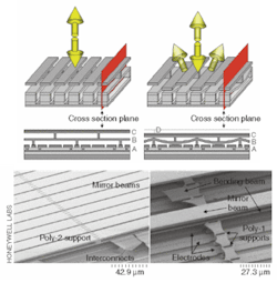
A prototypical diffractive MEMS chip of this configuration contains an array of flat, parallel mirror elements suspended on a structure that, when actuated, bends and lowers the mirror elements (see Fig. 1).4 In the unactuated state, light impinging at normal incidence is simply reflected back. However, when alternate beams are displaced, the device becomes an efficient diffractor of light, with correspondingly less light returned by reflection along the original incident direction. When the displacement is exactly one-quarter of the wavelength of the incident light, there is ideally no light reflected back; all the light is diffracted.
A unique characteristic of this approach is that, because of the double-layer structure, the actuated reflector surface remains flat and parallel to the substrate. The diffraction phenomenon depends on the respective difference in phase of the light reflected from the displaced and nondisplaced mirror elements. A flat, displaced mirror element will have uniform phase across its entire surface, thus providing a more nearly ideal extinction of the reflected light under quarter-wavelength actuation. This detail is exploited to achieve high dynamic range in both telecommunications and spectroscopic wavelength-management applications.
Wavelength management
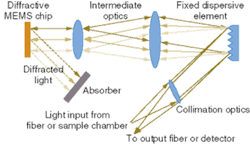
A diffractive MEMS chip can be used to build a wavelength-management device (see Fig. 2). Light is brought in either via an optical fiber or with free-space optics. This light is split into its constituent colors by a fixed diffraction grating, and then focused onto the MEMS chip. Each region, or pixel, of the MEMS chip receives a different band of wavelengths; by actuating that pixel, some of the light is diffracted away, reducing the amount of light returned by reflection.
FIGURE 2. In a diffractive-MEMS-based wavelength-management device, light spectrally split by a fixed grating is imaged onto the MEMS chip, which tailors the strength of all spectral elements ("wavelength management").
Unlike the device developed at Silicon Light Machines, which uses the diffracted light to form a display, in this architecture, it is the reflected zero-order light that is used. At exactly one-quarter wavelength of actuation, reflection from a pixel is (ideally) totally extinguished. In between zero actuation and one-quarter wavelength, there is complete analog control of the intensity of the reflected light in the wavelength band controlled by each pixel. The reflected light is redirected onto the fixed diffraction grating so that the light from each wavelength rejoins a single path close to the original incidence path. This recombined light is then either captured into an optical fiber or is directed onto a photodetector with additional optics. Thus, it is possible to build highly versatile programmable spectral filters—either fiber-to-fiber or source-to-detector—and it is this capability that forms the technology platform for the applications of interest.
Telecommunications applications
Optical networks that are already deployed were not designed to be automatically reconfigured. Provisioning additional wavelengths or routing them to a different location requires the replacement or redistribution of dozens of static components (for example, gain-flattening filters) that are applied to demultiplexed individual wavelengths and customized for a specific network state. This process costs a substantial amount of time and money and requires excessive manpower to alter the network configuration. Moreover, network management complexity grows significantly as new wavelengths are added. More than any other factor, these complexities are responsible for the long and complicated process of optical-network upgrades.
As diffractive MEMS devices can generate an arbitrary tunable filtering function across a spectral band, these structures are proving to be robust and flexible power-management enablers for telecommunications networks. Thus, a telecommunications carrier can adjust the power level of any individual optical channel anywhere from fully passing the wavelength to fully blocking it (a method used to reroute the wavelength to other directions in the network). Attenuated states are used to equalize the power across the spectral band and thus extend the optical network's reach at lower cost. Consequently, diffractive MEMS can form the fundamental building block for reconfigurable optical add/drop multiplexers. Carriers and systems manufacturers have begun to use diffractive MEMS as dynamic gain equalizers and wavelength blockers, and in emerging wavelength-selective-switch applications to address the limitations of today's static and inflexible architectures.
Spectroscopy applications
Optical spectroscopy is widely used for chemical analysis and monitoring of chemical processes. Each chemical species absorbs light at characteristic wavelengths. The conventional method of performing chemical identification is to measure the entire spectrum of transmitted light across some preselected range of wavelengths, and then to analyze the spectrum to identify characteristic absorption lines of target chemicals. One goal of modern instrumentation is to make such chemical-sensing measurements more efficient with respect to speed, the use of available light energy from the source, and cost, for example by using a single detector rather than an array.
Wavelength-management architecture enables a MEMS chip to be used to create various patterns of "off-on" filters, passing some bands and blocking others. A technique known as Hadamard-transform spectroscopy allows a complete spectrum to be collected with a single detector using a time sequence of filter patterns. Using a prototype MEMS chip, Sinclair and Pfeifer programmed the MEMS to implement this filter sequence and demonstrated a compact and efficient Hadamard spectrometer.5
A particularly important application is the analysis of mixtures of compounds. The generic name for the extraction of compound information from a mixture is "chemometrics."6 Chemometric analysis extracts a weighted sum of light absorbances at different wavelengths to perform the separation. This exact function can be performed in real time by the diffractive MEMS chip, creating a compact and versatile chemical-analysis system.
STEPHEN D. SENTURIA is chairman, chief technology officer, and cofounder, MOULI RAMANI is vice president of marketing and business development, and YARIV GELLER is director of business development at Polychromix, 30 Upton Dr., Wilmington, MA 01887; e-mail: [email protected].
REFERENCES
- O. Solgaard, F. S. A Sandejas, and D. M. Bloom, Optics Lett. 17, 688 (1992).
- R. Monteverde, Laser Focus World 40, 93 (January 2004).
- M. B. Sinclair, M. A. Butler, A. J. Ricco, and S. D. Senturia, Appl. Optics 36, 3342 (1997).
- G. B. Hocker et al., Proc. Solid-State Sensor and Actuator Workshop, 89 (Hilton Head, SC; June 4–8, 2000).
- M. B. Sinclair and K. B. Pfeifer, Materials Research Society Spring Meeting, San Francisco, CA, Symp. Materials, Mechanisms and Systems for Chem. and Biological Detection and Remediation, paper Y4.1 (April 14–15, 2004).
- M. Otto, Chemometrics, Meinheim: Wiley-VCH (1999).

