Over the past several years, work on organic light-emitting diodes (OLEDs) has overcome problems such as current injection, resulting in devices with total efficiencies higher than 10%. Most research has been focusing on ways to lengthen OLED lifetimes beyond about 50,000 hours by reducing degradation in the devices. A group from Stanford University (CA) is concentrating, instead, on increasing the light output of OLEDs—which might just lengthen OLED lifetimes, too.
FIGURE 1. A stamp of polydimethylsiloxane (PDMS; an elastomer) is made using holographic lithography (left). A drop of the conducting polymer PEDOT dispersed in water is placed on the stamp, which is then pressed down against the ITO electrode on the OLED substrate. As the water evaporates, the PEDOT forms a grating that enhances light extraction (right).
At the Fall Meeting of the Materials Research Society (Dec. 1–5, 2003; Boston, MA), Michael David McGehee presented work by his group on patterning the substrates of OLEDs to increase the light output.1 They made one- and two-dimensional Bragg gratings using a printing method that increased light output in the forward direction by 70%.
Although OLEDs can generate light with high efficiency, more than half of the light can be trapped in the device. In 2000, Ifor Samuel and others at University of St. Andrews (Fife, Scotland) demonstrated that Bragg gratings in the surface under the waveguide can couple light out of that plane, but the group never optimized the structure.2
Refining the design
McGehee's group took steps toward optimizing the structure for light output and developed a patterning method that will work in mass production. Whatever changes they made had to be possible without degrading the device's operating characteristics (such as turn-on voltage) and without substantially adding to the cost.
They incorporated Bragg gratings into the device by stamping the layer of polymer directly below the active layer. A very small amount of PEDOT (a conducting polymer that enhances hole injection into the active layer) is stamped onto the indium tin oxide (ITO) electrode (see Fig. 1). The grating depth ranges from 40 to 60 nm.
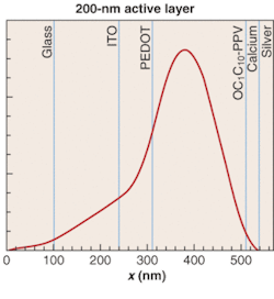
The researchers also changed the structure of the device slightly to enhance the action of the grating. A thicker active layer resulted in stronger waveguiding, more mode confinement, and higher fields in the grating region.
Still, light was being lost by reabsorption in the calcium of the upper electrode layer. "Everyone in the laser-diode community knows that metals in waveguides absorb a lot of light," McGehee explains. He notes that acting on this knowledge had not been necessary in the past for the OLED community. The layer of calcium in the OLED was thinned and augmented with silver, resulting in less absorption. An upcoming paper in Advanced Functional Materials describes the work more fully. Development continues as, for example, OLED companies insist that they would prefer aluminum to silver.
Concentrating on getting light out, McGehee says, "is the last opportunity to get a 2× to 5× enhancement in the brightness of OLEDs." By using the Bragg gratings to increase the efficiency of the output, the device's total quantum efficiency could approach 100%. "OLEDs with higher efficiencies are exciting because they run at lower currents," says McGehee. "This increases battery lifetime, prevents the OLEDs from heating up and prevents the OLEDs from degrading. Improving light extraction is a great way to indirectly address the degradation problem."
REFERENCES
- M. G. McGehee and J. Ziebarth, MRS Fall Meeting 2003, paper W6.9.
- J. M. Lupton et al., Appl. Phys. Lett. 77(21), 3340 (2000).

