Optical Systems: Transmissive high-energy laser optics: Manufacturing and testing considerations
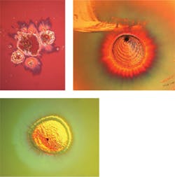
Optical substrates and coatings can fail mechanically when exposed to laser radiation of sufficient energy. These failure mechanisms include laser-induced dielectric breakdown and/or effects caused by significant heating. Since the advent of the laser, there has been a great deal of effort put into improving the performance of optical components exposed to ever-increasing laser energies (see Fig. 1).
The mechanisms of laser-induced damage are a function of factors specific to the laser, the application, the optical materials used, the optical manufacturing processes, and the use environment. In this article, we will discuss the general considerations for specifying, manufacturing, and testing antireflection (AR)-coated optics for high-energy laser (HEL) applications.
Specifying AR coatings for HEL applications
Antireflection coatings are applied to windows and lenses to reduce surface reflection and increase light transmission. These coatings typically consist of alternating high- and low-index-of-refraction layers, where each layer is a transparent dielectric film of thickness measured in nanometers.
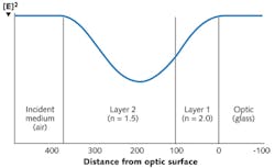
The coatings work through optical interference of light reflected from each interface within the layer stack. A standing-wave electric field is generated inside of the multilayer as a result of this interference (see Fig. 2).When specifying an antireflection coating, it is important to stipulate wavelength range, polarization, and the angle range of incident light. The system designer's goal for surface reflectivity should be included with the understanding that as wavelength range and angle range increase so does the minimum reflectivity that can be achieved.
There are different considerations for pulsed and continuous-wave (CW) lasers when specifying the required laser-induced damage threshold (LIDT). In pulsed laser systems, optical components often fail as a result of localized heating and/or dielectric breakdown associated with the peak fluence of the beam. A laser damage specification for a pulsed laser application should include the wavelength, pulse length, repetition rate, and required minimum energy fluence the component must survive (typically in J/cm2).
Optical coatings in CW systems typically fail because of heating and related thermal-mechanical effects. Failure in CW systems is usually not a function of peak energy but instead average power over a given area. In high-average-power laser systems optical designers must often consider both laser damage threshold and thermal distortion due to component heating. Laser damage threshold specifications for CW optical components are typically described in terms of power/area (typically W/cm2) after taking into account any localized hot spots in the beam.
For pulsed lasers with long pulse lengths or very high repetition rates the coatings can fail by either dielectric breakdown or through heating. It is therefore sometimes necessary for the designer to specify minimum requirements in terms of both average power and peak power for these systems.
Manufacturing considerations for HEL AR-coated surfaces
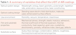
The LIDT of a given antireflection coating is influenced by a large number of variables. A summary of LIDT considerations in coating design and manufacturing are listed in Table 1. In this section, the influence of surface preparation, coating design, and material selection will be discussed.Surface preparation. The LIDT of an optical component used in transmission is strongly influenced by surface preparation. Oftentimes the ultimate LIDT of a transmitting element will be limited by how well the surface was polished and cleaned prior to coating. It is imperative that the substrate manufacturer use a carefully designed removal process in each grinding and polishing step. Each step should remove the residual surface cracks left by the preceding process with the ultimate goal of leaving a surface as free of subsurface damage as possible.
Flaws and residual surface cracks can act as both absorption sites and areas of locally intensified electric fields.1 Traces of residual polishing compound on or embedded in the optic can act as localized absorption sites that ultimately lead to failure. Careful selection of polishing compounds can minimize absorption due to trace contamination.2
Cleaning the optical surfaces is arguably the single most important step in achieving consistently high LIDTs on transmissive optics. The most effective final cleaning processes use an abrasive mechanical scrub, detergents, high purity solvents, repeated high-purity DI water rinses, and sometimes ultrasonic cleaning.3 Drying and transporting optics to the coating chamber are also critical steps; ideally the cleaning and coating facilities will both be located in cleanrooms to reduce possible contamination from airborne particulates.
Optical coating design. A common approach to improving LIDT of a multilayer high-reflection (HR) dielectric mirror coating is to design it so that the peak standing-wave electric field intensity is not located near damage-threshold-limiting features. It is standard practice to move peak electric fields away from areas of higher localized absorption (interfaces) and lower band gaps (high-index layers).4 AR-coated surfaces generally fail at lower energies than HR-coated surfaces because a higher percentage of incident intensity reaches the defect-laden substrate interface. AR coatings fail with higher probability on the exiting surface of an optic and, subsequently, damage testing is sometimes specified to be done through the glass.5
The mechanism of higher failure probability on the back surface is likely the result of multiple factors. Back surface Fresnel reflections, diffraction effects, beam self-focusing, and plasma interactions with the incident beam and coating have been investigated as potential contributors.6,7 For a perfect antireflection coating, there would be no electric field amplification due to back-surface Fresnel reflection. For an imperfect AR or uncoated optic, constructive interference of the reflected beam amplifies the field near the polished surface layer on the back of the optic.
Higher fields result in lower damage thresholds, especially in the vicinity of subsurface damage, contamination, and material boundaries. The same field amplification on the front surface would occur in incident air and would not be an issue.
Coating materials selection. In material selection for high LIDT coatings, there are often tradeoffs between optical design, material property, and manufacturing considerations. Coating designs would ideally include materials with low absorption, high band-gap energies, and no defects.
When designing an optical coating, it is often advantageous to have the largest spread possible between low- and high-index-of-refraction layers. Higher-index materials have lower band-gap energies and begin absorbing at longer wavelengths. As wavelength decreases so does availability of good nonabsorbing high-index materials.
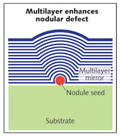
Absorption in a layer can be intrinsic or impurity-driven. The defects can be small (grain boundaries, oxygen deficiencies, pores, trace contamination) or relatively large (coating nodules). A nodule is an over-coated particle, typically caused by either airborne contamination or spatter due to dielectric breakdown in precursor coating materials. Micron-sized nodules (see Fig. 3) not only act as absorption sites but can enhance local electric fields through lensing.8Careful precursor material selection, conditioning, and processing can significantly reduce nodules. Functional pulsed laser damage thresholds are often defect-limited. For many CW applications failure results due to absorption over larger spatial areas in the coating and bulk thermal-mechanical properties of the films become more important.
Coating uniformity. Most optical-coating processes deposit coatings in a line of sight from the precursor material to the optic. Evaporation, plasma-ion assisted evaporation, and ion beam sputtering are all line-of-sight processes. It is possible to introduce low and mid-spatial frequency errors when depositing these coatings if no consideration for thickness uniformity is given during process and coating chamber design. These nonuniformities can cause changes in reflectance, transmittance, and phase.
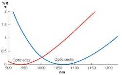
On curved surfaces, coating thickness is a function of chamber geometry, optic diameter, and the compound angle between the deposition source and optic surface at a point. Nonuniformity can become significant for optical coating performance as optic diameter increases and radius of curvature decreases. Figure 4 shows the effect of uncorrected nonuniformity on AR performance for a 150 mm radius of curvature convex lens with specified clear aperture of 100 mm in diameter. Reflectivity increases with distance from the lens center and, as previously discussed, so does field intensity in the optic at the exiting surface. The effect can become worse at higher angles of incidence.To address loss of transmission on curved surfaces Optimax Systems has developed software to model nonuniformity and a process to correct it. There are two options for dealing with nonuniformity. The first approach is to model nonuniformity and design a coating that is spectrally wide enough to accommodate the shift in center wavelength as coating thickness changes. These broader designs will give better transmitted performance across the entire lens, but a higher minimum reflectivity.
The second approach is to correct uniformity, which allows the coating designer to deposit a narrow design with the lowest absolute reflectivity across the entire clear aperture. Correcting uniformity can come at an additional expense as reduced batching efficiency is an unavoidable consequence of the process.
Testing considerations for CW applications
Modern pulsed-laser test sources can provide sufficient peak fluence to induce damage in most, if not all types of laser optics. For lasers working in CW mode, however, this is not the case. CW laser sources with the required brightness have been limited in power because of the cavity constraints needed to maintain good beam quality at high average power. A well-behaved beam is paramount when utilizing a laser damage test source because beam quality affects the repeatability and accuracy of the measurement.
This power limit requires the use of extremely small test spot sizes to reach typical damage-inducing irradiance levels. Small spots are not desirable because of the limited interaction area between the laser beam and the clear aperture of the optic under test. In a defect-driven damage model the threshold is driven by the distribution of defects on the sample. If the laser beam is small, the probability of interaction between the beam and the defect is reduced, and the result is often an artificially high apparent damage threshold.
Techniques like raster scanning help increase the irradiated area and can give results that are more representative of actual optic performance in use. The raster scanning approach does have some drawbacks. The testing times can be long, and the irradiation time on a singular site is not easily quantified in real time when the sample is moving.9 In addition, heat flow in an absorbing coating, which may be a driving factor in CW damage, can be significantly different for large and small beam radii.
With the advent of extremely high-power multimode fiber lasers, CW damage testing is now becoming an important tool in the development of downstream beam steering and focusing optics. These lasers have significant applications in material processing and the military.
Fortunately, the recent developments in high-power multimode fiber laser systems can be extended to single-mode laser systems with low divergence and excellent beam quality. These lasers make good sources for damage testing where stable power and repeatable beam quality are of paramount importance.
In support of these efforts, Spica Technologies has recently installed a 1 kW CW fiber laser for CW testing of optical components. This laser provides excellent beam quality (m2 =1.05) for near diffraction limited focusing, allowing CW peak irradiance levels in excess of 1 GW/cm2. In addition, the laser can be used to achieve high irradiance levels in large spots, providing for the interrogation of absorption and laser-induced surface figure change.
Acknowledgments
The authors would like to thank Dr. James Oliver, Dr. Semyon Papernov (University of Rochester Laboratory for Laser Energetics), and Justin Wolfe (Lawrence Livermore National Laboratory) for their helpful correspondences as related to the writing of this article.
References
1. N. Bloembergen, "Roles of cracks, pores, and absorbing inclusions on laser induced damage threshold at surfaces of transparent dielectrics," Appl. Opt. 12, 661–664 (1973)
2. R. Wood, Laser-induced Damage of Optical Materials, (IOP Publishing Ltd., 2003).
3. A.L. Rigatti, "Cleaning process versus laser damage threshold of coated optical components," in Frontiers in Optics 2004/Laser Science XXII/Diffractive Optics and Micro-Optics/Optical Fabrication and Testing, OSA Technical Digest (CD) (Optical Society of America, 2004), paper OMB3.
4. J. H. Apfel, "Optical coating design with reduced electric field intensity," Appl. Opt. 16, 1880 (1977).
5. R. Chow, M. Runkel, and J.R. Taylor, "Laser damage testing of small optics for the National Ignition Facility," Appl. Opt. 44, 3527–3531 (2005)
6. M. D. Crisp, N. L. Boling, and G. Dube, "Importance of Fresnel reflections in laser surface damage of transparent dielectrics,"Appl. Phys. Lett. 21, 364–366 (1972).
7. M.D. Feit, et al., "Modeling of laser damage initiated by surface contamination," Proc. SPIE 2966, 417–424 (1997).
8. C. Stolz, M. Feit and T. Pistor, "Laser intensification by spherical inclusions embedded within multilayer coatings," Appl. Opt. 45, 1594–1601 (2006).
9. M. R. Borden, J. A. Folta, C. J. Stolz, J. R. Taylor, and J. E. Wolfe, Lawrence Livermore National Laboratory; A.J. Griffin, M. D. Thomas, Spica Technologies Inc., "Improved Method for Laser Damage Testing Coated Optics," SPIE Boulder Damage Symposium, Oct. 2005.
Michael Thomas | President, Spica Technologies
Michael Thomas is president of Spica Technologies (Hollis, NH), and also chairs a committee under the Optics and Electro-Optics Standards Council (OEOSC) tasked to generate a new U.S. laser-damage standard for the measurement of laser damage on optical components.
Pete Kupinski | Optical Coating Group Leader, Optimax Systems
Pete Kupinski is optical coating group leader at Optimax Systems (Ontario, NY).
