Optical Tweezers: Plasmonic nanostructures are optimized for optical trapping
Optical trapping of microparticles at or near the focus of a laser beam via gradient forces has become useful in science, and in particular the life sciences, where biological cells can be held in place for sorting or experimentation. Creating an optimum focused beam for optical trapping is the object of intense research; one approach is to use plasmonic structures, including chiral structures (which have a right- or left-handed twist).
The use of arrays of nanoplasmonic structures enables a technique called self-induced back-action (SIBA) that allows reduced laser intensity, reducing potential damage to the trapped microparticles, as well as more options for handling and sorting. Saulius Juodkazis, professor of nanophotonics at Swinburne University of Technology (Melbourne, Australia), and his group have developed a plasma-etch procedure that easily produces these arrays for laser trapping and other uses.1,2
The Swinburne group numerically modeled and then experimentally checked the performance of a number of different types of arrayed plasmonic structures, including holes and wells. In one example, a computer simulation modeled a 100-nm-thick gold film on a glass substrate; the film was patterned with a lattice of 200-nm-diameter water-filled holes, with some versions converted into wells with the addition of rings at the tops of the holes.
The simulations modeled the optical power transmitted and reflected by the device; calculations were done on a 5 x 5 array of plasmonic structures, enclosed by so-called perfectly-matched layers and illuminated with a plane wave.
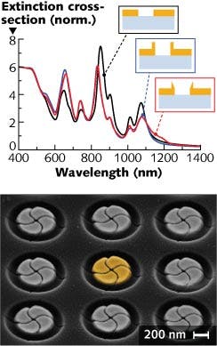
The researchers fabricated versions of the structures they modeled, including chiral and nonchiral nanostructures, then imaged the structures in array with a microscope. To capture the experimental transmission, reflection, and extinction spectra of the arrays, they coupled a Princeton Instruments (Acton, MA) IsoPlane spectrometer to the microscope; the spectrometer has a Czerny-Turner design with the addition of a Schmidt corrector, allowing the researchers to capture information across the arrays without aberrations.
The experimental normalized extinction cross-sections defined by the sum of absorption and scattering (see figure) show that adding sides to (nonchiral) holes to create wells reduced the transmission without overly affecting the spectral properties.
When the researchers modeled the force maps produced by the structures on a polystyrene-bead probe at 760 and 808 nm wavelengths in both water and air, they found that the best trapping conditions occurred for the conical nanowells at 760 nm.
Using plasmonic nanostructures for SERS
Other types of gold nanostructure arrays on glass substrates can be useful for sensitive detection of absorption and light scattering at low concentrations of analyte (in gas/air or solution) by surface-enhanced Raman scattering (SERS). The Swinburne group has created such arrays also, some with chiral structures. Optical characterization of these individual structures, as well as of arrays, via imaging (dark- and brightfield microscopy) along with spectral-extinction measurements provided the first and most informative evaluation of the fabricated patterns and individual nanoparticles.
The project is part of the Melbourne Center for Nanofabrication (MCN), the largest nanotechnology facility in the southern hemisphere.
REFERENCES
1. G. Gervinskas et al., Adv. Opt. Mat., 1, 6, 456 (2013).
2. G. Seniutinas et al., Beilstein J. Nanotechnol., 4, 534 (2013).

John Wallace | Senior Technical Editor (1998-2022)
John Wallace was with Laser Focus World for nearly 25 years, retiring in late June 2022. He obtained a bachelor's degree in mechanical engineering and physics at Rutgers University and a master's in optical engineering at the University of Rochester. Before becoming an editor, John worked as an engineer at RCA, Exxon, Eastman Kodak, and GCA Corporation.
