All-optical computers offer high speed and high levels of parallelism, but problems of miniaturization and manufacturability must be overcome to move ideas out of the laboratory.
Just as fiberoptic technology, with its tremendous speed and bandwidth, has largely replaced electronics in long-distance telecommunication networks, computer scientists have long strived to develop optical, or photonic, versions of electronic computers. Photons have significant potential advantages over electrons—they can interpenetrate each other unaltered, allowing the use of three-dimensional devices that are difficult or impossible to implement electronically, they are far more energy efficient, and, of course, they always move at the speed of light.
But researchers trying to make these potential advantages into realities face very significant challenges—optical-computing devices tend to be large and bulky, require careful alignment, and are not easy to miniaturize using existing photolithographic techniques. Such problems are just beginning to be addressed as researchers focus on basic system design ideas, but they are essential to moving technologies out of the laboratory.
Why optical computing?
While electronic computers have continued to advance in speed and memory at an exponential rate, doubling their clock rate every few years or so, there are inherent limitations in all electronic devices. First, electrons cannot move through each other nor can electric currents—they must always be directed through wires of some sort. This means, for example, that three-dimensional interconnections and three-dimensional computers have always been difficult to implement—there would be just too many crossconnecting wires and switches. Yet three-dimensional structures have inherent advantages in density of processing—a 1-cm cubic array of 1-µm transistors could theoretically contain a trillion transistors or the equivalent.
In addition, electrons inevitably generate heat as they move through conductors and semiconductors. This heat must be removed and puts potential limits on the density and speed of chips and multiprocessor computers. And, electronic devices operate at speeds far less than the speed of light. A typical clock step today is a few nanoseconds, but the time it takes light to get from one end of a chip to the other is a hundred times less.
Optical computers can potentially overcome all three disadvantages. Light can travel through free space without the need for wires or fibers, and photons can travel through each other without alteration. So optical computers can be designed that are inherently three-dimensional and highly parallel. Elements such as three-dimensional holograms can be accessed by many beams simultaneously, and with other interference effects entire memories can be queried instantaneously, not in serial fashion.
Furthermore, energy losses from light traversing free space are negligible, allowing highly energy-efficient devices. And while electro-optic switches can slow down optical computers, some optical computations, again using interference effects, can be performed literally at the speed of light.
But optical computing has serious obstacles, as well. It is difficult to fabricate optical elements that are very small, so most laboratory systems are bench-top-sized, not chip-sized. New techniques have been developed to implement optical elements with silicon photolithography, but they are still relatively immature. In addition, optical elements need tight tolerances to work. And while optical computing can in some cases do what electronic computing does, but better and faster, the truly unique, purely optical capabilities are just now being developed for computing applications.
Putting optical computing to work
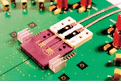
Given the strengths and weaknesses of optical computing, the main applications are not in replacing general-purpose electronic computers but in narrower niches in which optical advantages are the greatest. The most obvious of these are in interconnecting conventional electronic computer chips or boards (see photo). Potentially, optical interconnects can vastly increase connectivity and reduce communication times for machines with multiple processors.
A second important application area is in neural networks. These were first developed to imitate human and animal neural processing and involve self-learning networks for pattern recognition and image processing. Optical methods are ideal for neural networks because they are highly parallel and rely on every unit interacting with every other one. Similarly, shared memory, often in the form of holographic memories, is another way of exploiting the natural parallelism of optical techniques.
Although it is clearly a long-term goal, researchers are also looking at more-general systems of optical logic that could execute any arbitrary program that is implementable on a conventional chip. Even more exciting, a number of groups are looking at new ways of computing, using the quantum and interference properties of light to eliminate many of the intermediate steps involved in conventional Turing-machine computers.
Spatial light modulators
A crucial element of virtually any optical-computing system is a way to encode information efficiently on a lightwave. To take advantage of the three-dimensional nature of optical computing, such encoding is typically done by varying the amplitude or phase of a lightwave over a plane consisting of individuals modulators or "smart pixels." Such spatial light modulators (SLMs) can be electro-optical, in which an electrical signal is used to modulate the light wave, or purely optical, in which one light signal is used to modulate another.
Spatial light modulators use a variety of physical principles, essentially all those that are used in any kind of optical modulator. A simple example is a Mach-Zehnder interferometer, in which a beam is split in two and an electric field is applied to one optical path before the two are recombined. By varying the phase of one leg with the applied voltage, constructive or destructive interference can be selected. Using the Kerr effect, the same result can be obtained using an input light to change the refractive index of one leg, making an all-optical switch. Similarly, magneto-optical or acousto-optical effects can be used for other electro-optical SLMs.
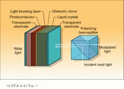
The most developed technology for arrays of spatial light modulators is liquid crystals, which are used in ubiquitous displays. In such liquid-crystal displays (LCDs), an electric field alters the polarization properties of the liquid-crystal molecules, either allowing or blocking light transmission. To create an all-optical switch, a photoconductive layer is added to a liquid-crystal cell. The "write" light signal, coming from one side, changes the potential on the photoconductive layer, thus creating a shift in the transmittance of the "read" lightwave coming from the opposite direction (see Fig. 1).Optical interconnects
The most obvious application for optical-computing technology is in board-to-board interconnects on large-scale parallel processors. In such interconnects, the smart-pixel arrays are driven by electronic commands from the parallel processor but use optical switching in free space to do the interconnection. Many of the early versions of such interconnects used a simple system with five elements. A square array of light sources such as LEDs or lasers is focused by a single lens onto a smart-pixel array that is modulated with the output from one board. A second lens images the output of the first array onto a detector array attached to the second board. This is the optical equivalent of hardwired connections.
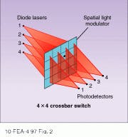
However, more sophisticated approaches are also being tried out. For example, SLMs combined with sets of cylindrical lenses can create cross-bar switches, connecting any output in a line with and input in another line (see Fig. 2). In this approach, a vertical cylindrical lens fans out the light from each modulated spot across a row of SLMs, while a second horizontal cylindrical lens focuses the outputs of the SLMs onto a row of detectors. In this way, if, say, all but one SLM is closed in a given row, that determines the connection between a single element in the line of emitters and the corresponding element in the line of detectors. An advantage of this device is that data from one output can be linked to several inputs instantly, or the outputs of several sources can be additively combined at a single input.Neural nets and image processing
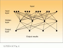
A second application in which the optical capability for many-to-many interconnections is highly desirable is in neural networks. Neural networks, very roughly based on biological models, are systems in which processing units are interconnected by different weighting functions, which alter in response to inputs. A typical neural network consists of three layers—an input layer, a hidden layer, and an output layer (see Fig. 3). Each processor or node "fires" in response to its inputs from the preceding layer, which are summed according to the system of weights. During training, "correct" responses, for example, identifying a given pattern correctly as an aircraft, lead to increased weights. Over time, the neural network adjusts its own weights, training itself to recognize patterns that are similar but not identical.Generally, such neural networks are simulated on conventional serial processors, which tend to make them operate slowly. Parallel electronic hardware implementation is impeded by the need to connect all nodes in one layer to all those in the next. With optics, all-to-all connections can be done diffractively. In optical neural networks, SLMs are used to create holograms that act as the interconnection between the layers of a neural network, distributing responses from an input pattern to an array of output detectors.
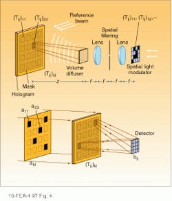
In the simplest systems, the creation of the hologram occurs off-line; each SLM element is exposed, together with a reference beam, to create a hologram (see Fig. 4). A diffuser spreads out the SLM image over the whole of the hologram. The weights of each element, representing an interconnection weight, are encoded by varying the exposure time of the hologram. Because an interconnection weight must be defined connecting each pixel in an N × N array with each pixel in another N × N array, N4 connections must be defined, while each N × N SLM array defines only N2. But in the system designed by Taiwei Lu and colleagues at Physical Optical Corp. (Torrance, CA), multiple exposures of the SLM are made by moving a mask on the hologram plane both horizontally and vertically, so that the final hologram contains N2 different images of SLM arrays, each representing the interconnection weights for a single node in one layer to all the nodes in a second layer.In operation, inputs, encoded by an SLM array, are directed onto the hologram, which then acts as an N4 switch, focusing the outputs with appropriate weights onto the N2 detector. For a 256 × 256 array, the device yields 4 billion interconnections, far beyond the capacity of any electronic hardware. A full-fledged neural network with three layers would have two separate holograms connecting the input to the hidden layer and the hidden layer to the output layer. A system using optical interconnects to connect the first two layers and electronic interconnections between smaller second and third layers successfully identified images of tanks, planes, and helicopters with arbitrary rotations after being trained (off-line) on images presented at various angles.
To train on-line, with the network modifying its own weights, holographic read-write memories are required. Such memories are now beginning to be developed by researchers for application in both neural networks and more-conventional computers.
The capabilities of such neural networks can potentially be expanded by using multiple frequencies of light as another dimension of information, in addition to the two spatial dimensions. Akira Hirose and Rolf Eckmiller of the University of Bonn`s Institute of Neuro informatics (Bonn, Germany) are working out schemes for such carrier-frequency-modulated neural networks with promising initial results. (Interestingly, there is some evidence that the human brain uses a sort of frequency-domain processing to coordinate the work of its hundreds of billions of cells, producing in some still-mysterious way a single perception out of a myriad of impulses and extremely low-frequency electromagnetic waves.)
Ideally, optical computers should be able to perform as general-purpose machines, substituting directly for electronic counterparts. There are a number of different avenues to this ambitious goal. Some groups of researchers are developing SLMs as direct equivalents of electronic gates. In general, these schemes use some combination of optical modulators and electronic circuits integrated onto a signal chip, but all-optical devices can be used as well. A typical design involves input beams focused on the pixels obliquely, and results read out perpendicular to the chip surface. Such direct substitutes could achieve speeds greater than those of electronic computers, but only with algorithms that can be made highly parallel, so that streams of information can be fed to every pixel equally.
Designing from scratch
An entirely different approach is to attempt to design optical computers from scratch, utilizing from the start the potentials of coherent light to access millions of pixels of data simultaneously. In the research of H. John Caulfield of Alabama A & M University (Normal, AL) for example, an effort is being made to develop computer instruction in the form of holographic interference patterns. Instead of performing parallel trains of sequential steps, arriving at many intermediate answers on the way to the final output, this scheme allows the interference pattern of photons passing through the holograms to "calculate" the final answer in a single pass, thus potentially achieving both great speed and low-energy operation.
To develop such novel schemes with the same general-purpose applicability as conventional electronic computers, however, will be the work of many more years of research. In the meantime, optical computing components will probably begin entering the market through more-specialized applications.
FURTHER READING
H. John Caulfield, Laser Focus World 31(5), 181 (May 1995).
A. Hirose and R. Eckmiller, Appl. Opt. 35, 836 (10 Feb. 1996).
T. Lu et al., Opt. Engineer. 35, 2122 (Aug. 1996).
