DANIEL H. RAGUIN and G. MICHAEL MORRIS
Diffractive optics reshape wavefronts, performing such tasks as focusing, collimating, and beamsplitting. Subwavelength-structured (SWS) surfaces, a less conventional type of diffractive optic, can mimic the effect of thin-film coatings, supplying antireflection, polarizing, or filtering effects. Such surfaces can be used for applications in which thin-film approaches are not viable.
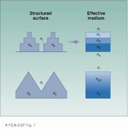
Subwavelength-structured surfaces operate on the principle that surface structure, rather than chemistry, can be used to synthesize an effective index of refraction for the surface layer. An SWS surface contains a surface-relief grating (phase or amplitude) in which the grating period is small compared to the wavelength of the incident light (typically l/2 or l/4), so that no diffractive orders other than the reflected and transmitted zeroth orders are allowed to propagate. The light does not experience diffraction effects; instead, it "sees" a homogeneous region with an effective index of refraction that is a combination of the indices of the substrate and incident medium (see Fig. 1).
The effective refractive index synthesized by an SWS surface can be quantified by effective-medium theories (EMTs).1 While mathematically simple and accurate enough to generate good first-order designs, EMTs are approximations. Once first-order design parameters are determined, the design should be finalized using a more rigorous vector diffraction theory.
Although EMTs are functions of the incident wavelength-to-period ratio and the indices of refraction of the materials involved, the critical manufacturing parameter (in terms of its effect upon the surface's effective index) is the filling factor f = a/L, where L is the period, and a is the width of the raised portion of the substrate. The filling factor specifies the fractional amount of substrate material contained within a grating period and is the key parameter to control when manufacturing SWS surfaces.
Optical holography provides an excellent means for the fabrication of large SWS surfaces. The substrate is coated with a layer of photoresist, which is exposed using a standard two-beam holographic grating setup. With proper exposure and development, deep one-dimensional (1-D) grating profiles in photoresist can be obtained. The patterned photoresist surface is then placed in a reactive-ion etcher, which transfers the grating surface into the substrate material. Two-dimensional (2-D) surface profiles can be created using a double-exposure technique in which the substrate is rotated by 90° between exposures, yielding a 2-D (or crossed) grating structure.
Antireflection and polarizing surfaces
Subwavelength-structured surfaces can be used as antireflection-structured surfaces (ARSs) for both polarized and unpolarized light. When properly designed, these structures can operate over large spectral bandwidths and large fields of view.2,3
To illustrate the performance that can be obtained using an ARS surface, consider the design of a quarter-wave antireflection coating. The conventional realization consists of a quarter-wave, index-matching thin-film layer. Although antireflection coatings are straightforward to design, practical issues can complicate the fabrication and performance. Materials with the required refractive index may be unavailable or may have undesirable properties (hygroscopic or carcinogenic). Mismatches between coefficients of thermal expansion for the thin film and substrate can render coatings vulnerable to thermal cycling. Coating materials can outgas under vacuum or fail to adhere to the substrate.
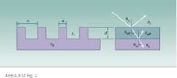
The structural approach skirts these difficulties. To form a quarter-wave ARS surface, a designer chooses a binary grating with a grating filling factor that yields an effective index of refraction of exactly nf = (nins)1/2. This grating pattern is then etched into the substrate material to a quarter-wave depth (see Fig. 2).
Because an ARS surface is formed directly in the substrate material, it does not suffer from many of the practical difficulties associated with thin-film coatings. Like any high-frequency grating surface, however, the surface-relief structure of an ARS surface should be protected; foreign materials such as water or oils that fill the grating structure will alter its properties. The surfaces are otherwise effective and are useful for applications in which thin-film solutions are not viable, such as those involving corrosive environments or repeated thermal cycling.
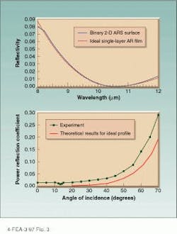
The SWS approach has been used to produce antireflective surfaces for infrared wavelengths from 8 to 12 µm. By etching a grating with a period of 2.45 µm along the x and y axes and a filling factor of 0.49 into a gallium arsenide (GaAs) substrate, engineers at Rochester Photonics Corp. (RPC; Rochester, NY) produced a surface with a single-layer effective refractive index of 1.81 at the design wavelength of 10.6 µm (see figure at top of this page). In experiments, the ARS performance was comparable to the theoretical performance of an ideal single-layer antireflection coating, whose index of refraction may not always exist in nature (see Fig. 3). Data from experiments showed good agreement with vector diffraction results for the ideal ARS surface.
Antireflection-structured surfaces can have either 1-D or 2-D profiles, which can be multilevel or continuous depending upon the design specifications that must be satisfied. The 2-D ARS surface discussed above is designed for use with unpolarized light; for polarized light, 1-D ARS surfaces are appropriate. Applications for either type include infrared windows and domes, detector surfaces, baffle systems, and optical signature control.
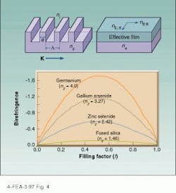
Subwavelength surfacing can impart a birefringent surface to any isotropic material that can be etched, replicated, or molded. The grating structure is fabricated with different filling factors along the x and y axes. Incident light polarized along the x direction sees an effective index of nx, while light polarized along the y direction sees an effective index of ny. The surface behaves as a negative uniaxial crystal with birefringence (Dn = nx - ny) an order of magnitude above that found in conventional materials such as quartz, calcite, and even cadmium sulfide. A 1-D surface provides the maximum amount of birefringence (see Fig. 4). Grating depth is usually quite small—typically less than the wavelength of the incident radiation.
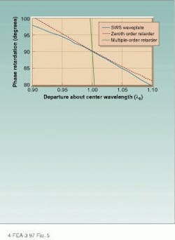
Engineers at RPC have fabricated an SWS zinc sulfide quarter-wave plate for CO2 laser applications (see Fig. 5). Such an element simulates the performance of a conventional zeroth-order phase retarder and is relatively insensitive to detunings from the design wavelength. SWS elements can also be used to fabricate other polarization elements such as polarizing mirrors, wire-grid polarizers, and beamsplitters.
Narrowband filters
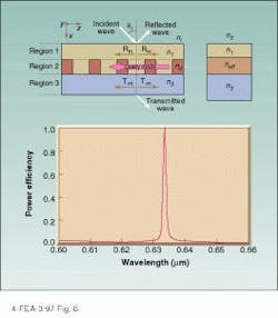
Subwavelength-structured surfaces can act as narrowband filters in which the reflection spectra of the surface change rapidly as a function of incident wavelength or incident angle.4-7 The basic design consists of a grating sandwiched between a substrate and a cover layer that also fills the grooves of the grating (see Fig. 6). When the effective index of refraction of the grating region is greater than that of the substrate or the cover, a waveguide is created.
When the filter is designed properly, incident light passes into this waveguide region and propagates as a leaky mode. The grating structure of the region selectively couples light at a narrow band of wavelengths or incident angles into the waveguide. This light propagates a very short distance—on the order of tens to hundreds of microns—undergoes scatter, and couples with the forward- and backward-propagating zeroth-order light. This highly sensitive coupling condition can produce the resonant grating effect on the reflected radiation spectrum.
A number of degrees of freedom allow designers to tailor filter performance. Layer thickness is used to obtain symmetric line shapes and low sideband reflection. Grating duty cycle is used to control the spectral linewidth, and grating period is used to select the center wavelength. In practice, peak reflectivities in the range of 60% to 90% have been achieved with FWHMs ranging from 0.1 to 10 nm. The reflectivities and linewidths of SWS filters equal or exceed those obtained using conventional thin-film stacks consisting of 50 to 60 thin-film layers.
Subwavelength-structured surfaces can produce very efficient antireflection and polarizing elements, as well as narrowband filters for the visible and infrared spectral regions. With the recent improvements in holographic fabrication methods and submicron lithography, production of SWS surfaces is now commercially viable.
REFERENCES
1. S. M. Rytov, Soviet Phys. JETP 2, 466 (1956).
2. D. H. Raguin and G. M. Morris, Appl. Opt. 32, 1154 (1993).
3. D. H. Raguin and G. M. Morris, Appl. Opt. 32, 2582 (1993).
4. R. Magnusson and S. S. Wang, Appl. Phys. Lett. 61, 1022 (1992).
5. M. T. Gale, K. Knop, and R. Morf, Proc. SPIE 1210, 83 (1990).
6. S. Peng and G. M. Morris, J. Opt. Soc. Am. 13, 993 (1996).
7. S. Peng and G. M. Morris, Opt. Lett. 21, 549 (1996).
Daniel H. Raguin is vice president of research and development and G. Michael Morris is chief executive officer at Rochester Photonics Corp., 330 Clay Road, Rochester, NY 14623; Morris is also a professor at The Institute of Optics, University of Rochester, Rochester, NY; e-mail: [email protected]; [email protected].

