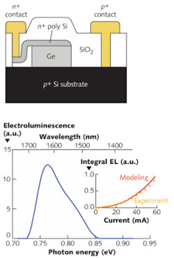
The last few years have seen a surge in the development of silicon-based photonic components. Despite successful fabrication of silicon routers, modulators, waveguides, switches, silicon photodiodes, and even hybrid silicon lasers, an all-silicon laser integrated with silicon photonic components still proves elusive. As the debate rages over the correct roadmap for achieving a silicon photonics inter- and intrachip network, research groups are making progress in developing a true electrically injected silicon light source.
In addition to the recent demonstration of a 4.2 mW electrically pumped hybrid evanescent silicon/indium gallium arsenide phosphide (Si/InGaAsP) laser by researchers at the California Institute of Technology (Caltech; Pasadena, CA), researchers at the Massachusetts Institute of Technology (MIT; Cambridge, MA) have successfully fabricated monolithically integrated germanium-on-silicon (Ge-on-Si) light-emitting diodes (LEDs) that display direct-bandgap electroluminescence at room temperature.1, 2
Better than a silicon hybrid
Although electrical injection is possible in 1550 nm hybrid III-V Si lasers either bonded to a Si waveguide or grown on Si-based buffer layers, fabrication costs are high, making high-volume manufacture difficult. A better approach is a monolithically integrated emitter that is compatible with complementary metal-oxide semiconductor (CMOS) fabrication processes—precisely what is delivered by the Ge-on-Si LEDs developed by the MIT team.
Unlike Si, Ge has a direct bandgap only slightly larger than its indirect bandgap (by 0.136 eV), which can be engineered to inject electrons in the direct valley of the conduction band radiatively recombining with holes with very little loss from nonradiative processes. The observed direct-gap photoluminescence is boosted by introducing in-plane biaxial tensile stress into epitaxial Ge thin films on Si. Because calculations show that Ge becomes a 0.5 eV (2500 nm) direct-bandgap material at tensile strain values of 2%, a smaller strain value of 0.20% to 0.25% is introduced that yields a bandgap around the telecommunication wavelength of 1550 nm with better materials quality and reliability.
Devices were fabricated by growing epitaxial Ge on boron-doped Si substrates. A silicon dioxide (SiO2) layer deposited on the substrate was patterned to expose regions for the subsequent Ge growth (see figure). Post-growth thermal annealing to relax the 1.7-µm-thick Ge layer was followed by room-temperature cooling to introduce the 0.20% tensile strain. Polysilicon was added as a final coating, along with n and p contacts.
Applying an electrical injection current of 50 mA to a 20 × 100 µm device produced optical emission around the direct-bandgap energy of 0.77 eV (or 1610 nm)—the first observation, to the researchers’ knowledge, of direct-gap electroluminescence from any Ge device. This direct-gap electroluminescence exhibits a super-linear relationship with the injected electrical current, making Ge-on-Si devices promising candidates for electrically pumped and efficient monolithic light emitters on Si.
“Germanium has never seriously been pursued as a potential efficient light emitter on Si until very recently,” says MIT research scientist Xiaochen Sun. “MIT’s extensive investigation of tensile-strained Ge leads to the realization of Ge LEDs. Further engineering and optimization will be carried out to increase the performance by orders of magnitude aiming for milliwatts-on-chip light emitters,” he adds.
REFERENCES
- X.Sun et al., Optics Lett. 34(9) p. 1345 (May 1, 2009).
- X. Sun et al., Optics Lett. 34(8) p. 1198 (April 15, 2009).

Gail Overton | Senior Editor (2004-2020)
Gail has more than 30 years of engineering, marketing, product management, and editorial experience in the photonics and optical communications industry. Before joining the staff at Laser Focus World in 2004, she held many product management and product marketing roles in the fiber-optics industry, most notably at Hughes (El Segundo, CA), GTE Labs (Waltham, MA), Corning (Corning, NY), Photon Kinetics (Beaverton, OR), and Newport Corporation (Irvine, CA). During her marketing career, Gail published articles in WDM Solutions and Sensors magazine and traveled internationally to conduct product and sales training. Gail received her BS degree in physics, with an emphasis in optics, from San Diego State University in San Diego, CA in May 1986.